Electrical Engineering (EE) Exam  >  Electrical Engineering (EE) Tests  >  SSC JE Electrical Mock Test Series 2025  >  Test: Basic Electronics- 3 - Electrical Engineering (EE) MCQ

Test: Basic Electronics- 3 - Electrical Engineering (EE) MCQ


Test Description

20 Questions MCQ Test SSC JE Electrical Mock Test Series 2025 - Test: Basic Electronics- 3

Test: Basic Electronics- 3 for Electrical Engineering (EE) 2024 is part of SSC JE Electrical Mock Test Series 2025 preparation. The Test: Basic Electronics- 3 questions and answers have been prepared according to the Electrical Engineering (EE) exam syllabus.The Test: Basic Electronics- 3 MCQs are made for Electrical Engineering (EE) 2024 Exam. Find important definitions, questions, notes, meanings, examples, exercises, MCQs and online tests for Test: Basic Electronics- 3 below.
Solutions of Test: Basic Electronics- 3 questions in English are available as part of our SSC JE Electrical Mock Test Series 2025 for Electrical Engineering (EE) & Test: Basic Electronics- 3 solutions in Hindi for SSC JE Electrical Mock Test Series 2025 course. Download more important topics, notes, lectures and mock test series for Electrical Engineering (EE) Exam by signing up for free. Attempt Test: Basic Electronics- 3 | 20 questions in 12 minutes | Mock test for Electrical Engineering (EE) preparation | Free important questions MCQ to study SSC JE Electrical Mock Test Series 2025 for Electrical Engineering (EE) Exam | Download free PDF with solutions
Test: Basic Electronics- 3 - Question 1

Generally, mobility of electrons in semiconductor is _________ times the mobility of holes:

Detailed Solution for Test: Basic Electronics- 3 - Question 1

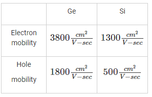
Mobility of electrons and holes depends on their effective masses. Effective mass of electrons is less than that of holes hence electrons have higher mobility than holes.

For both Ge & Si μe > 2μh

Hence option (b) is correct.

Test: Basic Electronics- 3 - Question 2

In a p-n Junction with no externally applied voltage, the drift and diffusion components of the hole and electron currents:

Detailed Solution for Test: Basic Electronics- 3 - Question 2

In a p-n Junction when no bias voltage is applied, the net current is zero.

Hence the drift and diffusion components of the hole and electron currents must sum to zero.

1 Crore+ students have signed up on EduRev. Have you? Download the App
Test: Basic Electronics- 3 - Question 3

Fermi level is the measure of

Detailed Solution for Test: Basic Electronics- 3 - Question 3

From the definition of fermi level, the fermi level is energy state having probability ‘1/2’ of being occupied by an electron.

Test: Basic Electronics- 3 - Question 4

Semiconductor lasers are based on the following principle:

Detailed Solution for Test: Basic Electronics- 3 - Question 4

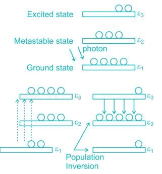
LASER stands for Light Amplification by Stimulated Emission of Radiation. These are based on the principle of population inversion at a junction as explained in below figure

Test: Basic Electronics- 3 - Question 5

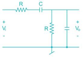
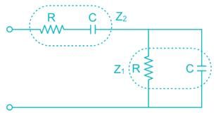
The circuit shown in the figure is a:

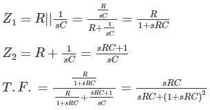
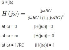
Detailed Solution for Test: Basic Electronics- 3 - Question 5


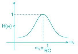
The frequency Response is shown


Bandpass filters at ω0 = 1/RC

Test: Basic Electronics- 3 - Question 6

The capacitance of a p-n junction diode:

Detailed Solution for Test: Basic Electronics- 3 - Question 6

During forward Bias, the diffusion capacitance is the dominant capacitance.

τ = mean lifetime of minority carriers

If = forward current

As forward current Increase exponentially,

The junction capacitance increases exponentially on forward bias.

Test: Basic Electronics- 3 - Question 7

A light-emitting diode (LED) converts:

Detailed Solution for Test: Basic Electronics- 3 - Question 7

LED works on the principle of electroluminescence which is emission of light under influence of electric field.

Test: Basic Electronics- 3 - Question 8

A Bipolar Junction Transistor saturation point may be defined as

Detailed Solution for Test: Basic Electronics- 3 - Question 8

For a BJT operating in active mode, the base current (Ib) and collector current (IC) are related as Ic = β Ib where β is the current gain.

At saturation the voltage across collector – emitter junction (VCE) is constant (∼ 0.2V) and collector current is independent of base current.

Test: Basic Electronics- 3 - Question 9

In a rectifier, commutation of diodes refers to transferring energy from –

Detailed Solution for Test: Basic Electronics- 3 - Question 9

Commutation in a rectifier is the process of transfer of current from one device (diode or thyristor) to the other in a rectifier. The device from which the current is transferred is called the outgoing device and the device to which the current is transferred is called the incoming device. The incoming device turns on at the beginning of commutation while the outgoing device turns off at the end of commutation.

Here, commutation of diodes refers to transferring energy from rectifier diode to freewheeling diode. Freewheeling diode is used to reduce the harmonics and also suppress the voltage spikes occur in inductive load.

Test: Basic Electronics- 3 - Question 10

Which among the following has a frequency selective amplifier whose gain decreases from a finite value to zero as the frequency of the sinusoidal input increase form dc to infinity?

Detailed Solution for Test: Basic Electronics- 3 - Question 10

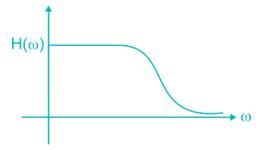
The frequency response of LPF is shown

From the frequency response it is clear that the gain of low pass filter decreases form finite value to zero as frequency is increased from 0 to ∞

Test: Basic Electronics- 3 - Question 11

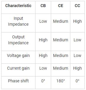
Consider the following circuit configurations:

1. Common emitter

2. Common base

3. Emitter follower

The correct sequence in increasing input impedance is 

Detailed Solution for Test: Basic Electronics- 3 - Question 11

Test: Basic Electronics- 3 - Question 12

In a bipolar junction transistor, the current gain β.

Detailed Solution for Test: Basic Electronics- 3 - Question 12


The current gain β is defined as 

At higher temperatures the thermal injection increases the collector current & hence β increases.

Test: Basic Electronics- 3 - Question 13

The h-parameter equivalent circuit of a BJT is valid for:

Detailed Solution for Test: Basic Electronics- 3 - Question 13

The h-parameters model doesn’t take into account junction capacitance which are significant at high frequencies. The h-parameter model is valid for signals with Vbe < 10 mV. Hence h-parameter model is suitable for low frequencies & small signals

Test: Basic Electronics- 3 - Question 14

Transistors leakage current mainly depends on:

Detailed Solution for Test: Basic Electronics- 3 - Question 14

The leakage current in a transistor mainly depends on temperature and doubles for every 10°C rise in temperature. This leakage current dependence on temperature is responsible for thermal run-away in transistors.

Test: Basic Electronics- 3 - Question 15

The base region of a p – n – p transistor is:

Detailed Solution for Test: Basic Electronics- 3 - Question 15

In pnp transistor, the base is n-type semiconductor i.e. it is doped with electrons. The width of the base region is kept small/thin to allow maximum carriers from emitter to pass through base to collector without much recombination

Test: Basic Electronics- 3 - Question 16

A transistor is said to be in a quiescent stage when

Detailed Solution for Test: Basic Electronics- 3 - Question 16

The Q-point in the Transistor is established for faithful Amplification in middle of DC-load line. The Q-point is established using DC voltage & resistance without any application of AC signal.

Test: Basic Electronics- 3 - Question 17

In a BJT, collector region width is maximum when it.

1. Collects maximum number of charge carrier

2. Reduces heat dissipation per unit area Out of these

Detailed Solution for Test: Basic Electronics- 3 - Question 17

The order of width is

wcollector > wemitter > wBase

The order of doping is

nemitter > ncollector > nbase

Test: Basic Electronics- 3 - Question 18

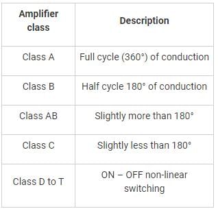
DC bias is adjusted greater than its cut-off value so that the output current flow for less than half of the input voltage cycle, in:

Detailed Solution for Test: Basic Electronics- 3 - Question 18

Test: Basic Electronics- 3 - Question 19

A tuned amplifier is used:

Detailed Solution for Test: Basic Electronics- 3 - Question 19

Tuned amplifiers are employed for the purpose of selecting a particular frequency among set of available frequencies. Hence they are employed in radio receives.

Test: Basic Electronics- 3 - Question 20

What is the required connection for an enhancement type N-MOSFET to function as a resistor?

Detailed Solution for Test: Basic Electronics- 3 - Question 20

The overdrive voltage is defined as the voltage between transistor gate and source (VGS) in excess of the threshold voltage (VT) ie Vgs - Vt

For N-Mos to function as a resistor, it should be operated in linear region. I.e. VDS < Vgs – Vt

For using N-Mos as an amplifier, it should be operated in saturation region. I.e. VDS ≥ Vgs – Vt

2 videos|1 docs|55 tests
Information about Test: Basic Electronics- 3 Page
In this test you can find the Exam questions for Test: Basic Electronics- 3 solved & explained in the simplest way possible. Besides giving Questions and answers for Test: Basic Electronics- 3, EduRev gives you an ample number of Online tests for practice

Top Courses for Electrical Engineering (EE)

Download as PDF

Top Courses for Electrical Engineering (EE)