Electrical Engineering (EE) Exam  >  Electrical Engineering (EE) Tests  >  Digital Electronics  >  Test: CMOS - 2 - Electrical Engineering (EE) MCQ

Test: CMOS - 2 - Electrical Engineering (EE) MCQ


Test Description

10 Questions MCQ Test Digital Electronics - Test: CMOS - 2

Test: CMOS - 2 for Electrical Engineering (EE) 2024 is part of Digital Electronics preparation. The Test: CMOS - 2 questions and answers have been prepared according to the Electrical Engineering (EE) exam syllabus.The Test: CMOS - 2 MCQs are made for Electrical Engineering (EE) 2024 Exam. Find important definitions, questions, notes, meanings, examples, exercises, MCQs and online tests for Test: CMOS - 2 below.
Solutions of Test: CMOS - 2 questions in English are available as part of our Digital Electronics for Electrical Engineering (EE) & Test: CMOS - 2 solutions in Hindi for Digital Electronics course. Download more important topics, notes, lectures and mock test series for Electrical Engineering (EE) Exam by signing up for free. Attempt Test: CMOS - 2 | 10 questions in 30 minutes | Mock test for Electrical Engineering (EE) preparation | Free important questions MCQ to study Digital Electronics for Electrical Engineering (EE) Exam | Download free PDF with solutions
Test: CMOS - 2 - Question 1

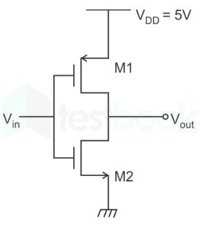
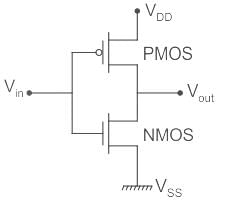
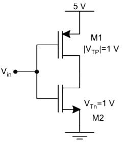
In the CMOS circuit shown, electron and hole mobilities are equal, and M1 and M2 are equally sized. The device M1 is in the linear region if
Detailed Solution for Test: CMOS - 2 - Question 1


M1 will be in linear region if Vout>Vin + VT

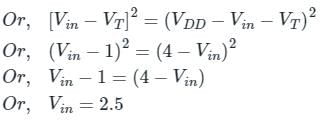
At the edge of the linear region Vout= Vin + VT


So, for Vin< 2.5 the PMOS will be in a linear region so the correct option is (1)

Test: CMOS - 2 - Question 2

When there is no clock signal applied to CMOS logic circuits, they are referred to as

Detailed Solution for Test: CMOS - 2 - Question 2

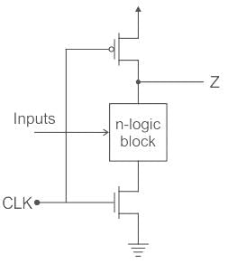
The circuit of a CMOS Logic circuit is as shown:

  • It is a simple single dynamic CMOS with Precharge phase CLK = 0 and Evaluate phase CLK = 1.
  • When no clock signal is applied, CMOS Logic circuit falls under static circuits in which every point in time, each gate output is connected to either VDD or VSS.
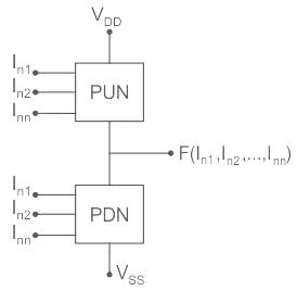
  • A static CMOS logic circuit is a combination of two networks, called the pull-up-network (PUN) & pull-down-network (PDN) as shown:
1 Crore+ students have signed up on EduRev. Have you? Download the App
Test: CMOS - 2 - Question 3

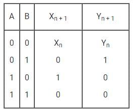
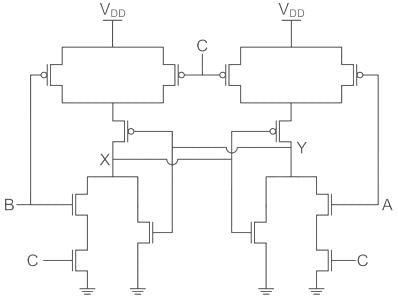
The following CMOS transistor based circuit with A, B, C as input and X, Y as output
Detailed Solution for Test: CMOS - 2 - Question 3

C is the clock signal
Consider C = 1
The truth table is


→ A = 1 and B = 1 is Forbidden
Whenever A = 1, Y = 0
Yn+1 = 0
Whenever B = 1, X = 0
XN+1 = 0
X = Q output
Y = Q̅ output
B = Reset (R)
A = Set (S)

Test: CMOS - 2 - Question 4

A digital CMOS IC operating at 10 MHz clock frequency consumes 100 mW power; the same IC operating at 15 MHz clock frequency consumes 140mW power. What is the static power consumption of the IC?

Detailed Solution for Test: CMOS - 2 - Question 4

Concept:
Static power is proportional to the static current, i.e. the current that flows regardless of gate switching.
Dynamic Power is related to the current that flows when switching takes place and is given by for CMOS as:

P = fCV2cc
Or P = Kf (where K = Vcc2C)
Power consumed by CMOS = Pstatic + Pdynamic

Calculation:
For f1 = 10MHz, Pconsumed = 100 mW = P1 (Let)
For f2 = 15MHz, Pconsumed = 140 mW = P2
⇒ P1 = Pstatic + Pdynamic
⇒ 100 mW = Pstatic + Kf1
⇒ 100 mW = Pstatic + K(10 M) …1)
Similarly, P2 = 140 mW = Pstatic + K(15 M) …2)
From equation (i) and (ii)
Pstatic = 20 mW

Test: CMOS - 2 - Question 5

In CMOS implementation of a NAND gate:

Detailed Solution for Test: CMOS - 2 - Question 5

CMOS is a combination of NMOS & PMOS.
NAND gate can be implemented using two PMOS in parallel and two NMOS in series as shown:

Observations:

  • When VA & VB are high at +VDD (5V), then the PMOS will be open-circuited and two NMOS will be short-circuited, the output will be short-circuited to ground and produces a Zero (0V) output.
  • When any of the input is low (0 V), the corresponding PMOS will be shorted and NMOS will be open, the output is shorted to VDD, i.e. it produces a high output.

NAND Gate:

It is the combination of AND Gate followed by NOT Gate.
When the two inputs A and B are high, then output y is low, otherwise, it is high.

Test: CMOS - 2 - Question 6

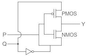
For the circuit shown in the figure, P and Q are the inputs and Y is the output.
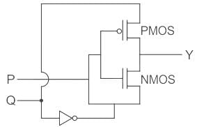
The logic implemented by the circuit is

Detailed Solution for Test: CMOS - 2 - Question 6

⇒ If P = high:
PMOS is OFF
NMOS is ON 
then y = Q̅
⇒If P = low
PMOS is ON
NMOS is OFF 
then  y = Q
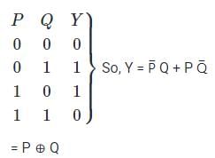
The truth table of the above will be as shown:

So, Ex – OR Operation is being performed.

Test: CMOS - 2 - Question 7

Which circuit takes the less chip area in large scale integration?

Detailed Solution for Test: CMOS - 2 - Question 7

In large scale integration (LSI), CMOS (complementary Metal-oxide Semiconductor) circuit takes the less Chip area during fabrication. This is because the CMOS circuit is a combination of NMOS and PMOS and it is fabricated as a twin tub process where the required Chip area is less.
During the process of bipolar logic families (such as RTL, DTCL, DTL, HTL, TTL, and ECL) fabrication, required large chip area as these circuits consist of NPN and PNP transistor, diodes, resistors, etc.
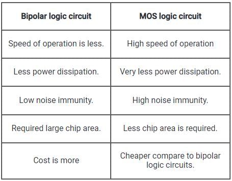
Important Comparison between bipolar logic circuits and MOS logic circuits:

Test: CMOS - 2 - Question 8

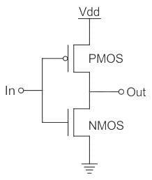
The above circuit acts as:

Detailed Solution for Test: CMOS - 2 - Question 8

Inverter

  • This is equal to NOT gate in the digital circuitry.
  • The output of this is a compliment of the input.


This can be built from the transistors like BJT, MOSFET, etc…

The CMOS inverter consists of the NMOS and the PMOS field-effect transistors connected in one below the other.


When In = Low
PMOS will be shorted and output will be High.
When In = High
NMOS will be shorted and output will be Low.
Hence it acts as an inverter.

Test: CMOS - 2 - Question 9

For a typical CMOS process, the minimum feature size is set to be 25 μm. The minimum line width at the process is set to be ______

Detailed Solution for Test: CMOS - 2 - Question 9

Concept:

  • Feature Size: The minimum feature size is the size or the width at which a transistor or any type of material on the silicon surface can be drawn at.
  • If the minimum feature size can be reduced, this means that the transistor length can be reduced effectively making the transistor smaller with the same electrical properties.
  • This allows for lower current flow between the junction for the same purpose and lesser heat dissipation.

The minimum line width is 2 × minimum feature size  ---(1)

Calculation:
Given:
Minimum feature size = 25 μm
Now the minimum line width can be calculated from equation (1)
Minimum line width = 2 × 25 μm
Minimum line width = 50 μm 
Hence option (3) is the correct answer.

Test: CMOS - 2 - Question 10

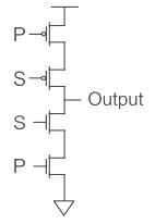
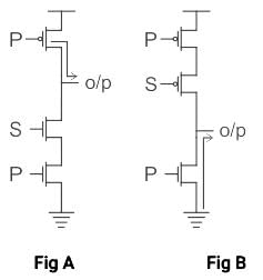
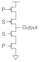
Output of the circuit shown below when S = 1 and S = 0 will be _____.
Detailed Solution for Test: CMOS - 2 - Question 10

Concept:
Complementary Metal-oxide-semiconductor (CMOS) uses complementary & symmetrical pair of P-type & n-type MOSFETS.

  • The two important characteristics of CMOS devices are high noise immunity and low power dissipation.
  • In CMOS, during static operation at a time, only one MOS is ON i.e. either PMOS or NMOS. So there is no direct path from the power supply to the ground. Hence, Power dissipation in CMOS is low in static operation but it has high power dissipation in dynamic operation.

Calculation:
As the given figure is of CMOS with two inputs.

The upper part is PMOS which is switched on when 0 is applied and NMOS is switched on when 1 is applied.


  • When S = 0 is applied, the PMOS connected to S (upper one) will be shorted and P at PMOS will appear across the output in complemented form as shown in fig(A).
    So Output = P̅
  • Now when S = 1 is applied, the NMOS connected to S (lower one) will be shorted, and due to which ground will appear across the output and the circuit will go in a high impedance state as shown in fig(B).

Hence option (2) is the correct answer.

115 videos|71 docs|58 tests
Information about Test: CMOS - 2 Page
In this test you can find the Exam questions for Test: CMOS - 2 solved & explained in the simplest way possible. Besides giving Questions and answers for Test: CMOS - 2, EduRev gives you an ample number of Online tests for practice

Top Courses for Electrical Engineering (EE)

115 videos|71 docs|58 tests
Download as PDF

Top Courses for Electrical Engineering (EE)