Test: EDC & Analog - Electronics and Communication Engineering (ECE) MCQ
25 Questions MCQ Test - Test: EDC & Analog

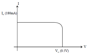
The figure Shows V-I charactertics of a solar cell illuminated uniformly with solar light of power 100mW/cm2. The solar cell has an area of 3cm2 and a fill factor of 0.7. The maximum efficiency of cell is
In the circuit shown below, assume that the diodes D1 and D2 are ideal. The average value of voltage Vab (in
volts) across the terminals a and b is
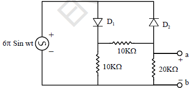
volts) across the terminals a and b is

Consider an n-type semiconductor in which the dopant concentration ND is 1014/cm3. If the intrinsic concentration of semiconductor 1010/cm3 then the concentration of electrons (n) and holes (P) at equillibrium are
Consider the following statements:
1. Fermi level in a p-type semiconductor lies close to the top of the valence band.
2. The forbidden energy in Germanium at 0 K is exactly 0.78 eV.
3. When a p-n junction is reverse biased, then electrons and holes move away from the junction.
Which of these statements are correct?

The junction capacitance of an abrupt pn junction is 10 pf at a reverse bias voltage of 3 volt. Determine the value of capacitance when a reverse bias voltage of 15 volt is applied, if the built in potential of junction is 1 volt.
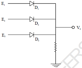
In the circuit shown, diodes D1, D2 and D3 are ideal and the inputs E1, E2 and E3 are 0 V for logic ‘0’ and 5V for logic ‘1’. What logic gate does the circuit represent?
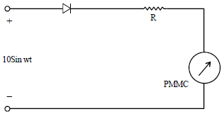
In the given circuit, the moving-coil meter gives full-scale deflection reading when the average current
flowing through it is 1mA. The moving coil meter has internal resistance of 50?. Find the value of R that results meter a full scale deflection.
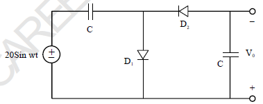
Assume both the diodes and both the capacitors are ideal. The value of V0 in steady state is
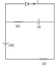
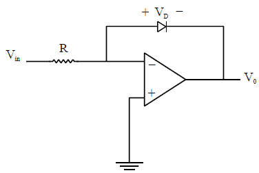
Assume the diode is ideal, determine the current ‘i’ in the given circuit.
Consider the following statements.
1. The PIV in a HWR with capacitive filter becomes 2 Vm
2. Ripple voltage is decreases as we increases the time period of input ac signal.
3. Conduction time of diode is decreases as we increase the value of capacitor.
Which of the following is/are correct?
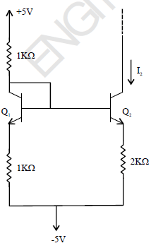
In the given circuit both the transistors are perfectly matched the value fo I2 is
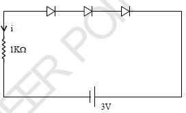
The forward threshold voltage of each diode in the given circuit is 1 Volt and reverse breakdown voltage of each diode is 10 Volt. Determine ‘i’
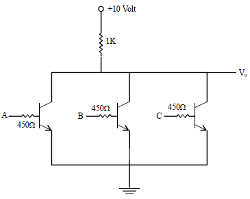
In the given circuit the VCE (sat) for each transistor is 0. The inputs A, B and C are 0 for logic 0 and they
are 5V for logic 1. The logic gate realized by the circuit. Assume β = 100
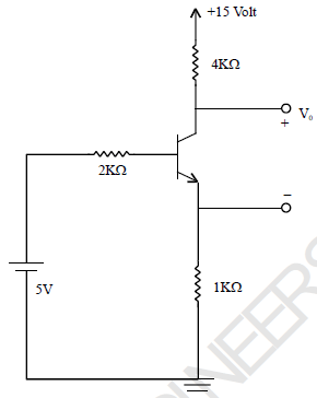
Assume β of the transistor is 100, determine the value of V0 in the given circuit.
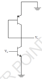
In the ac circuit shown {The DC biasing circuit is omitted), the two BJTs are biased in active region and
have identical parameters with β >> 1. The open circuit small signal voltage gain is approximately.
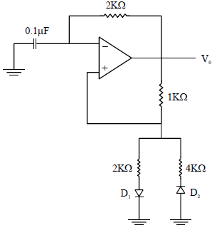
In the circuit shown below, assume both the diodes and opamp are ideal. Determine the frequency of the oscillation of the signal obtained at V0.
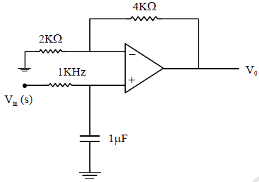
In the given circuit, assume opamp is ideal. Determine the type and 3-dB frequency of the filter.
For the CMOS circuit shown below the parameters for the MOSFET are given below:
For NMOS : Vth = 0.7V,
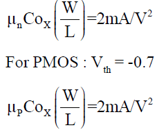
Determine region of MOSFET M1 and M2.
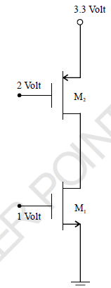
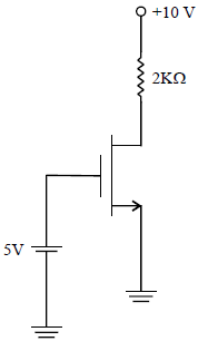
For the MOSFET shown in the circuit below has Vth = 1 Volt,
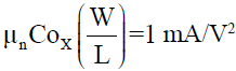 . Determine the resistance offered by the MOSFET.
Which of the following statement is not correct about a power amplifier?
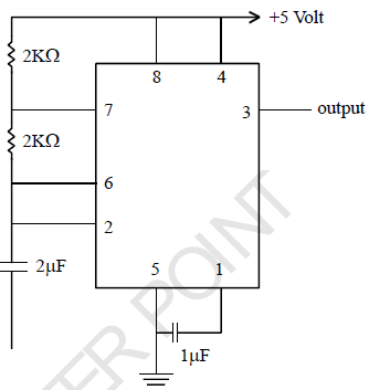
Determine the duty cycle of the square wave generated at the output of terminal 3:
A light of wavelength 4000A is incident on a semiconductor material having energy band gap is 1.4eV and electron hole pairs are generated. Determine the velocity of electron that is generated due to this illumination.
In the given circuit the opamp is ideal.
This circuit is popularly known as,
Adding an emitter resistor to a common-emitter amplifier causes:
A non-inverting op-amp is shown below {assume ideal op-amp}. For
Vin = (2 + Sin 100t) Volt
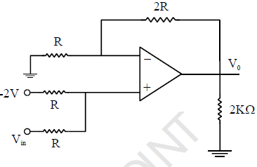
The output voltage V0 for an input
Important Questions for EDC & Analog
EDC & Analog MCQs with Answers
Online Tests for EDC & Analog
|
© EduRev
|
Education Revolution
|


|


