Electronics and Communication Engineering (ECE) Exam  >  Electronics and Communication Engineering (ECE) Tests  >  GATE ECE (Electronics) Mock Test Series 2025  >  Test: Electronic Devices - 4 - Electronics and Communication Engineering (ECE) MCQ

Test: Electronic Devices - 4 - Electronics and Communication Engineering (ECE) MCQ


Test Description

10 Questions MCQ Test GATE ECE (Electronics) Mock Test Series 2025 - Test: Electronic Devices - 4

Test: Electronic Devices - 4 for Electronics and Communication Engineering (ECE) 2024 is part of GATE ECE (Electronics) Mock Test Series 2025 preparation. The Test: Electronic Devices - 4 questions and answers have been prepared according to the Electronics and Communication Engineering (ECE) exam syllabus.The Test: Electronic Devices - 4 MCQs are made for Electronics and Communication Engineering (ECE) 2024 Exam. Find important definitions, questions, notes, meanings, examples, exercises, MCQs and online tests for Test: Electronic Devices - 4 below.
Solutions of Test: Electronic Devices - 4 questions in English are available as part of our GATE ECE (Electronics) Mock Test Series 2025 for Electronics and Communication Engineering (ECE) & Test: Electronic Devices - 4 solutions in Hindi for GATE ECE (Electronics) Mock Test Series 2025 course. Download more important topics, notes, lectures and mock test series for Electronics and Communication Engineering (ECE) Exam by signing up for free. Attempt Test: Electronic Devices - 4 | 10 questions in 30 minutes | Mock test for Electronics and Communication Engineering (ECE) preparation | Free important questions MCQ to study GATE ECE (Electronics) Mock Test Series 2025 for Electronics and Communication Engineering (ECE) Exam | Download free PDF with solutions
Test: Electronic Devices - 4 - Question 1

For a single stage BJT common base amplifier.

Detailed Solution for Test: Electronic Devices - 4 - Question 1


∴ Voltage gain can be greater than unity but current gain is always less than unity.

*Answer can only contain numeric values
Test: Electronic Devices - 4 - Question 2

A bipolar transistor has an emitter current of 1 mA. The emitter injection efficiency is 0.99, base transit factor is 0.995 and depletion region recombination factor of 0.998. The base current flowing through the transistor is _____μA.


Detailed Solution for Test: Electronic Devices - 4 - Question 2

The common emitter current gain is given by:

α = γ ∗ β ∗ δ

= 0.99 × 0.995 × 0.998 = 0.983

Collector current

Ic = αIE = 0.983 mA

Base current

IB = IE – IC

= 17 μA 

1 Crore+ students have signed up on EduRev. Have you? Download the App
*Answer can only contain numeric values
Test: Electronic Devices - 4 - Question 3

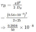
In a Bi-polar junction transistor the base width is 0.54 μm and base diffusion constant is DB = 25 cm2/sec. The Base transit time time is ________ × 10-10 sec


Detailed Solution for Test: Electronic Devices - 4 - Question 3

The Base transit time

⇒ 0.5832 × 10⁻¹⁰

*Answer can only contain numeric values
Test: Electronic Devices - 4 - Question 4

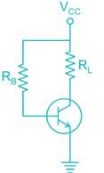
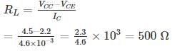
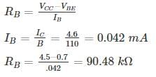
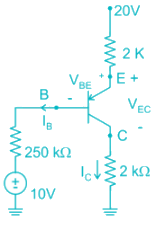
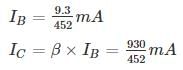
Find the value of bias resistor (in kΩ) if quiescent collector current and voltage value are 4.6 mA and 2.2 V. The transistor has DC gain 110, VBE = 0.7 V and VCC = 4.5 V.


Detailed Solution for Test: Electronic Devices - 4 - Question 4

Applying KVL in collector to emitter loop

VCC = RLIC + VCE


Now applying KVL in collector to base loop

IBRB + VBE = VCC

Test: Electronic Devices - 4 - Question 5

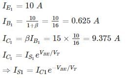
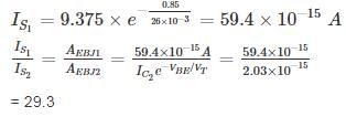
Consider two pnp bipolar junction transistors. For the first transistor when emitter to collector voltage is 5 V, VEB is 0.85 V and emitter current is 10 A. (The β for this transistor is 15). Second BJT conducts with a collector current of 1 mA and VEB = 0.70. The ratio of emitter-base junction area of the first transistor to the second transistor is ______.

(Assume KT = 26 mV)

Detailed Solution for Test: Electronic Devices - 4 - Question 5

Given: VEC = 5V-, this means pnp transistor is operating in the active node

*Answer can only contain numeric values
Test: Electronic Devices - 4 - Question 6

The leakage current of a transistor with usual notation are ICEO = 410 μA, ICBO = 5 μA, and IB = 30μA. Calculate the IC ________mA


Detailed Solution for Test: Electronic Devices - 4 - Question 6

ICEO = 410 μA, ICBO = 5 μA, IB = 30 μA

IC­ = βIB + (1 + β) ICBO

ICEO = (1 + β) ICBO

410 = (1 + β)5

β = 81

IC = 81 × 30 + 82 × 5

IC = 2.84 mA

Test: Electronic Devices - 4 - Question 7

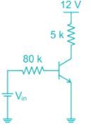
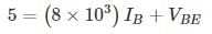
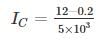
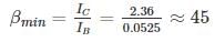
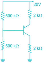
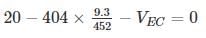
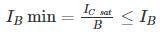
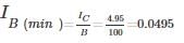
For what value of current gain β , the given transistor will be in saturation

(Assume Vin = 5V, VBE(SAT) = 0.8 V , VCE(SAT) = 0.2V)

Detailed Solution for Test: Electronic Devices - 4 - Question 7

Apply kVL in base emitter loop

at saturation VBE(sat) = 0.8

substituting the value of VBE

IB = 0.0525 mA

Apply Kvl , Form the collector to emitter

5 × 10³ × I+ VCE = 12 V

= 2.36 mA

At the edge of saturation

Hence for β value greater than 45 the transistor will be in saturation

*Answer can only contain numeric values
Test: Electronic Devices - 4 - Question 8

An npn bipolar transistor having uniform doping of NE = 1018 cm-3 NB = 1016 cm-3 and NC = 6 × 1015 cm-3 is operating in the inverse-active mode with VBE = -2V and VBC = 0.6 V. The geometry of transistor is shown

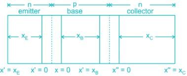
The minority carrier concentration at x = xB is _____ × 1014 cm-3

(Assume n = 1.5 × 10¹⁰/cm3, Vt ­= 25 mV)


Detailed Solution for Test: Electronic Devices - 4 - Question 8


= 5.96 × 1014 cm-3

Test: Electronic Devices - 4 - Question 9

The common emitter forward current gain of the transistor shown is β = 100
The transistor is operating in

Detailed Solution for Test: Electronic Devices - 4 - Question 9


Assume Transistor in Active region

20 – 2 (IB + IC) – 0.7 – 250 IB – 10 = 0

20 – 2 × 101 IB – 0.7 – 250 IB – 10 = 0

10 – 452 IB – 0.7 = 0

20 – 2 (IB + IC) - VEC – 2IC = 0

20 – 202 IB - VEC = 0


VEC = 11.68 V

VCB = VCE + VEB = -VEC + VEB = - 11.68 + .7

VCB = -10.98

∴ Collector base junction is Reverse Biased

∴ Transistor is operating in forward active region


Second Method

Assume transistor in saturation region

IB min ≤ IB

i) VEB (sat) = 0.8 V

ii) VEC (sat) = 0.2 V


IC ≠ βIB ----- Because it is valid only active region

20 – 2 (IB + IC) – 0.8 - 250 IB – 10 = 0

20 – 2 IB – 2IC – 0.8 – 250 IB – 10 = 0

10 – 252 IB – 2IC – 0.8 = 0

252 IB + 2I= 9.2      -------- (1)

20 – 2 (IB + IC) – VEC(sat) – 2IC = 0

20 – 2IB – 2IC – 0.2 – 2IC = 19.8      -------- (2)

By solving equation (1) and (2)

IB = 0.00278 mA

IC = 4.95 mA

∴ IB(min) > IB

∴ Transistor is operating in forward active region

Test: Electronic Devices - 4 - Question 10

In a silicon PNP transistor the mobility of charge carries is μ4 = 1300 cm2/V-s and μp = 450 cm2/V-s and carrier life time τp = 0.10 μs. The most appropriate base width for effective transistor function is (Take T = 300° k)
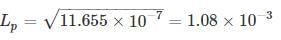
Detailed Solution for Test: Electronic Devices - 4 - Question 10

Given μn = 1300 cm2/V-s and μp = 450 cm2/V-s

Dp = 450 × 0.0259

= 11.655 cm2/s

Base diffusion length  = 1.08 mm

For injected holes from emitter to reach the collector they should not be recombined in base. Hence the base width should be very less compared to base diffusion length.

W ≪ LP

In all options the base width is significant compared to base diffusion length.

25 docs|263 tests
Information about Test: Electronic Devices - 4 Page
In this test you can find the Exam questions for Test: Electronic Devices - 4 solved & explained in the simplest way possible. Besides giving Questions and answers for Test: Electronic Devices - 4, EduRev gives you an ample number of Online tests for practice

Top Courses for Electronics and Communication Engineering (ECE)

Download as PDF

Top Courses for Electronics and Communication Engineering (ECE)