Electrical Engineering (EE) Exam > Electrical Engineering (EE) Tests > Test: Logic Families - 1 - Electrical Engineering (EE) MCQ
Test: Logic Families - 1 - Electrical Engineering (EE) MCQ
Test Description
10 Questions MCQ Test - Test: Logic Families - 1
Test: Logic Families - 1 for Electrical Engineering (EE) 2025 is part of Electrical Engineering (EE) preparation. The Test: Logic Families - 1 questions and answers have been prepared
according to the Electrical Engineering (EE) exam syllabus.The Test: Logic Families - 1 MCQs are made for Electrical Engineering (EE) 2025 Exam.
Find important definitions, questions, notes, meanings, examples, exercises, MCQs and online tests for Test: Logic Families - 1 below.
Solutions of Test: Logic Families - 1 questions in English are available as part of our course for Electrical Engineering (EE) & Test: Logic Families - 1 solutions in
Hindi for Electrical Engineering (EE) course.
Download more important topics, notes, lectures and mock test series for Electrical Engineering (EE) Exam by signing up for free. Attempt Test: Logic Families - 1 | 10 questions in 30 minutes | Mock test for Electrical Engineering (EE) preparation | Free important questions MCQ to study for Electrical Engineering (EE) Exam | Download free PDF with solutions

Detailed Solution for Test: Logic Families - 1 - Question 1
Test: Logic Families - 1 - Question 2
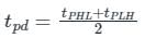
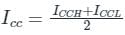
The figure of merit of a logic family is given by the product of:
Detailed Solution for Test: Logic Families - 1 - Question 2

Test: Logic Families - 1 - Question 3
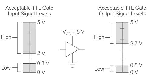
Two voltage given as -2 V and -1 V in positive logic convention represent:
Detailed Solution for Test: Logic Families - 1 - Question 3
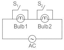
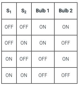
Detailed Solution for Test: Logic Families - 1 - Question 4
Detailed Solution for Test: Logic Families - 1 - Question 5
Test: Logic Families - 1 - Question 6
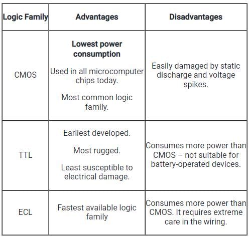
Which of the following does not belong to TTL subclasses?
Detailed Solution for Test: Logic Families - 1 - Question 6
Test: Logic Families - 1 - Question 7
A Darlington emitter-follower circuit is sometimes used in the output stage of a TTL gate in order to
Detailed Solution for Test: Logic Families - 1 - Question 7
Detailed Solution for Test: Logic Families - 1 - Question 8
Detailed Solution for Test: Logic Families - 1 - Question 9
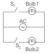
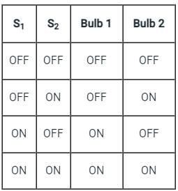
Test: Logic Families - 1 - Question 10
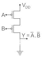
The logic function f(X,Y) realized by the given circuit is
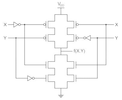
Detailed Solution for Test: Logic Families - 1 - Question 10
Information about Test: Logic Families - 1 Page
In this test you can find the Exam questions for Test: Logic Families - 1 solved & explained in the simplest way possible.
Besides giving Questions and answers for Test: Logic Families - 1, EduRev gives you an ample number of Online tests for practice
Download as PDF
Important Questions for Logic Families - 1
Find all the important questions for Logic Families - 1 at EduRev.Get fully prepared for Logic Families - 1 with EduRev's comprehensive question bank and test resources.
Our platform offers a diverse range of question papers covering various topics within the Logic Families - 1 syllabus.
Whether you need to review specific subjects or assess your overall readiness, EduRev has you covered.
The questions are designed to challenge you and help you gain confidence in tackling the actual exam.
Maximize your chances of success by utilizing EduRev's extensive collection of Logic Families - 1 resources.
Logic Families - 1 MCQs with Answers
Prepare for the Logic Families - 1 within the Electrical Engineering (EE) exam with comprehensive MCQs and answers at EduRev.
Our platform offers a wide range of practice papers, question papers, and mock tests to familiarize you with the exam pattern and syllabus.
Access the best books, study materials, and notes curated by toppers to enhance your preparation.
Stay updated with the exam date and receive expert preparation tips and paper analysis.
Visit EduRev's official website today and access a wealth of videos and coaching resources to excel in your exam.
Online Tests for Logic Families - 1
Practice with a wide array of question papers that follow the exam pattern and syllabus.
Our platform offers a user-friendly interface, allowing you to track your progress and identify areas for improvement.
Access detailed solutions and explanations for each test to enhance your understanding of concepts.
With EduRev's Online Tests, you can build confidence, boost your performance, and ace Logic Families - 1 with ease.
Join thousands of successful students who have benefited from our trusted online resources.
|
© EduRev
|
Education Revolution
|


|


Signup on EduRev and stay on top of your study goals
10M+ students crushing their study goals daily