Electronics and Communication Engineering (ECE) Exam  >  Electronics and Communication Engineering (ECE) Tests  >  Analog Circuits  >  Test: MOSFET In Amplifier Design - Electronics and Communication Engineering (ECE) MCQ

Test: MOSFET In Amplifier Design - Electronics and Communication Engineering (ECE) MCQ


Test Description

10 Questions MCQ Test Analog Circuits - Test: MOSFET In Amplifier Design

Test: MOSFET In Amplifier Design for Electronics and Communication Engineering (ECE) 2024 is part of Analog Circuits preparation. The Test: MOSFET In Amplifier Design questions and answers have been prepared according to the Electronics and Communication Engineering (ECE) exam syllabus.The Test: MOSFET In Amplifier Design MCQs are made for Electronics and Communication Engineering (ECE) 2024 Exam. Find important definitions, questions, notes, meanings, examples, exercises, MCQs and online tests for Test: MOSFET In Amplifier Design below.
Solutions of Test: MOSFET In Amplifier Design questions in English are available as part of our Analog Circuits for Electronics and Communication Engineering (ECE) & Test: MOSFET In Amplifier Design solutions in Hindi for Analog Circuits course. Download more important topics, notes, lectures and mock test series for Electronics and Communication Engineering (ECE) Exam by signing up for free. Attempt Test: MOSFET In Amplifier Design | 10 questions in 10 minutes | Mock test for Electronics and Communication Engineering (ECE) preparation | Free important questions MCQ to study Analog Circuits for Electronics and Communication Engineering (ECE) Exam | Download free PDF with solutions
Test: MOSFET In Amplifier Design - Question 1

(Q.1 & Q.2) Various measurements are made on an NMOS amplifier for which the drain resistor RD is 20 kΩ. First, DC measurements show the voltage across the drain resistor, VRD, to be 2 V and the gate-to-source bias voltage to be 1.2 V. Then, ac measurements with small signals show the voltage gain to be −10 V/V.

Q. What is the value of Vt for this transistor?

Test: MOSFET In Amplifier Design - Question 2

If the process transconductance parameter is 50μA/V2, what is the MOSFET’s W/L?

1 Crore+ students have signed up on EduRev. Have you? Download the App
Test: MOSFET In Amplifier Design - Question 3

(Q.3-Q.5) Consider the amplifier below for the case VDD = 5 V, RD = 24 kΩ, (W/L) = 1 mA/V2, and Vt = 1 V.
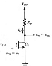
If the amplifier is biased to operate with an overdrive voltage VOV of 0.5 V, find the incremental gain at the bias point.

Test: MOSFET In Amplifier Design - Question 4

For amplifier biased to operate with an overdrive voltage of 0.5V, and disregarding the distortion caused by the MOSFET’s square-law characteristic, what is the largest amplitude of a sine-wave voltage signal that can be applied at the input while the transistor remains in saturation?

Detailed Solution for Test: MOSFET In Amplifier Design - Question 4

 Use the standard mathematical formula to obtain the result.

Test: MOSFET In Amplifier Design - Question 5

 For the input signal of 1.5V what is the value of the gain value obtained?

Detailed Solution for Test: MOSFET In Amplifier Design - Question 5

The amplitude of the output voltage signal that results is approximately equal to Voq – VOB = 2 – 0.61 = 1.39v.
The gain implied by amplitude is
Gain = -1.39/0.11 = -12.64 V/V.

Test: MOSFET In Amplifier Design - Question 6

Which of the following is the fastest switching device?

Detailed Solution for Test: MOSFET In Amplifier Design - Question 6

MOSFET is the fastest switching device among the given four options.

Test: MOSFET In Amplifier Design - Question 7

Bias point is also referred by the name

Detailed Solution for Test: MOSFET In Amplifier Design - Question 7

Bias point is called dc operating point as the MOSFET functions best at this point. Also since at the bias point no signal component is present it is called quiescent point (he reason why it is represented by the symbol ‘Q’)

Test: MOSFET In Amplifier Design - Question 8

(Q.8 –Q.10) Consider the amplifier circuit shown below. The transistor is specified to have Vt = 0.4 V, kn = 0.4 mA/V2, W/L = 10 and λ = 0. Also, let VDD = 1.8V, RD = 17.5kΩ, VGS = 0.6V and vgs = 0V.

Q. Find ID.

Test: MOSFET In Amplifier Design - Question 9

Find VDS.

Test: MOSFET In Amplifier Design - Question 10

 Find Av.

Detailed Solution for Test: MOSFET In Amplifier Design - Question 10

Av = – kn Vov RD
= -0.4 * 10 * 0.2 * 17.5
= – 14.4v

3 videos|33 docs|64 tests
Information about Test: MOSFET In Amplifier Design Page
In this test you can find the Exam questions for Test: MOSFET In Amplifier Design solved & explained in the simplest way possible. Besides giving Questions and answers for Test: MOSFET In Amplifier Design, EduRev gives you an ample number of Online tests for practice

Top Courses for Electronics and Communication Engineering (ECE)

3 videos|33 docs|64 tests
Download as PDF

Top Courses for Electronics and Communication Engineering (ECE)