Electrical Engineering (EE) Exam  >  Electrical Engineering (EE) Tests  >  GATE Electrical Engineering (EE) Mock Test Series 2025  >  Test: Microprocessor & Digital Logic Families - Electrical Engineering (EE) MCQ

Test: Microprocessor & Digital Logic Families - Electrical Engineering (EE) MCQ


Test Description

15 Questions MCQ Test GATE Electrical Engineering (EE) Mock Test Series 2025 - Test: Microprocessor & Digital Logic Families

Test: Microprocessor & Digital Logic Families for Electrical Engineering (EE) 2024 is part of GATE Electrical Engineering (EE) Mock Test Series 2025 preparation. The Test: Microprocessor & Digital Logic Families questions and answers have been prepared according to the Electrical Engineering (EE) exam syllabus.The Test: Microprocessor & Digital Logic Families MCQs are made for Electrical Engineering (EE) 2024 Exam. Find important definitions, questions, notes, meanings, examples, exercises, MCQs and online tests for Test: Microprocessor & Digital Logic Families below.
Solutions of Test: Microprocessor & Digital Logic Families questions in English are available as part of our GATE Electrical Engineering (EE) Mock Test Series 2025 for Electrical Engineering (EE) & Test: Microprocessor & Digital Logic Families solutions in Hindi for GATE Electrical Engineering (EE) Mock Test Series 2025 course. Download more important topics, notes, lectures and mock test series for Electrical Engineering (EE) Exam by signing up for free. Attempt Test: Microprocessor & Digital Logic Families | 15 questions in 45 minutes | Mock test for Electrical Engineering (EE) preparation | Free important questions MCQ to study GATE Electrical Engineering (EE) Mock Test Series 2025 for Electrical Engineering (EE) Exam | Download free PDF with solutions
Test: Microprocessor & Digital Logic Families - Question 1

Consider the following program of 8085 assembly language:
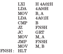
If the contents of memory location 4A00H, 4A01H and 4A02H, are respectively A7H, 98H and 47H, then after the execution of program contents of memory location 4A02H will be respectively

Detailed Solution for Test: Microprocessor & Digital Logic Families - Question 1

GRT : MOV M, B
FNSH : HLT

This program find the larger of the two number stored in location 4A00H and 4A01H and store it in memory location 4A002.

A7H > 98H Thus A7H will be stored at 4A02H.

Test: Microprocessor & Digital Logic Families - Question 2

Consider the following program of 8085 assembly language:

Que: The memory requirement for this program is

Detailed Solution for Test: Microprocessor & Digital Logic Families - Question 2

Operand R, M or implied : 1–Byte instruction
Operand 8–bit : 2–Byte instruction
Operand 16–bit : 3–Byte instruction

3–Byte instruction are: LXI, LDA, JZ, JC, JMP
P–Byte instruction are : MOV, CMP, HLT

Hence memory = 3 x 6 + 1 x 5 = 23 bytes

1 Crore+ students have signed up on EduRev. Have you? Download the App
Test: Microprocessor & Digital Logic Families - Question 3

The instruction, that does not clear the accumulator of 8085, is

Detailed Solution for Test: Microprocessor & Digital Logic Families - Question 3

All instruction clear the accumulator

Test: Microprocessor & Digital Logic Families - Question 4

Consider the following loop

             XRA     A
             LXI       B, 0007H
LOOP : DCX     B
             JNZ      LOOP

This loop will be executed

Detailed Solution for Test: Microprocessor & Digital Logic Families - Question 4

The instruction XRA will set the Z flag. LXI and DCX does not alter the flag. Hence this loop will be executed 1 times.

Test: Microprocessor & Digital Logic Families - Question 5

How many address bits are needed to select all memory locations in the 2118 16K × 1 RAM?

Test: Microprocessor & Digital Logic Families - Question 6

The contents of accumulator after the execution of following instruction will be 

MVI      A, A7H
ORA    A
RLC

Detailed Solution for Test: Microprocessor & Digital Logic Families - Question 6

The contents of bit D7 are placed in bit D0

Test: Microprocessor & Digital Logic Families - Question 7

The contents of accumulator after the execution of following instructions will be

MVI      A, B7H
ORA     A
RAL

Detailed Solution for Test: Microprocessor & Digital Logic Families - Question 7

RAL instruction rotate the accumulator left through carry.

Test: Microprocessor & Digital Logic Families - Question 8

The contents of the accumulator after the execution of the following program will be

MVI        A, C5H
ORA       A
RAL

Detailed Solution for Test: Microprocessor & Digital Logic Families - Question 8

RRC instruction rotate the accumulator right and D0 is placed in D7 .

Test: Microprocessor & Digital Logic Families - Question 9

Consider the following set of instruction

If BYTE1 = 07H, then content of A, after the execution of program will be

Detailed Solution for Test: Microprocessor & Digital Logic Families - Question 9

This program multiply BYTE1 by 10. Hence content of A will be 46H.

07H = 0710 , 7 x 10 = 70, 7010 = 46H

Test: Microprocessor & Digital Logic Families - Question 10

Consider the following program

MVI      A,BYTE1
RRC
RRC

If BYTE1 = 32H, the contents of A after the execution of program will be

Detailed Solution for Test: Microprocessor & Digital Logic Families - Question 10

Contents of Accumulator A = 0011 0010

After First RRC = 0001 1001
After second RRC = 1000 1100


Test: Microprocessor & Digital Logic Families - Question 11

The circuit shown in fig. is

Detailed Solution for Test: Microprocessor & Digital Logic Families - Question 11

If either one or both the inputs are V(0) = 0 V the corresponding FET will be OFF, the voltage across the load FET will be 0 V, hence the output is VDD . If boths inputs are V(1) = VDD, both M1 and M2 are ON and the output is V(0) = 0 V. It satisfy NAND gate.

Test: Microprocessor & Digital Logic Families - Question 12

The circuit shown in fig. acts as a

Detailed Solution for Test: Microprocessor & Digital Logic Families - Question 12

If both the inputs are at V(0) = 0 V, the transistor M1 and M2 are OFF, hence the output is V(1) = VDD  . If either one or both of the inputs are at V(1) = VDD  , the corresponding FET will be ON and the output will be V (0) = 0 V. Hence it is a NOR gate.

Test: Microprocessor & Digital Logic Families - Question 13

The circuit shown in fig.  implements the function

Detailed Solution for Test: Microprocessor & Digital Logic Families - Question 13

If all inputs A, B and C are HIGH, then input to invertor is LOW and output Y is HIGH. If all inputs are LOW, then input to inverter is also LOW and output Y is HIGH. In all other case the input to inverter is HIGH and output Y is LOW.

Test: Microprocessor & Digital Logic Families - Question 14

The circuit shown in fig. implements the function

Detailed Solution for Test: Microprocessor & Digital Logic Families - Question 14

The operation of circuit is given below

Test: Microprocessor & Digital Logic Families - Question 15

Consider the CMOS circuit shown in fig. The output Y is

Detailed Solution for Test: Microprocessor & Digital Logic Families - Question 15

The operation of this circuit is given below :

25 docs|247 tests
Information about Test: Microprocessor & Digital Logic Families Page
In this test you can find the Exam questions for Test: Microprocessor & Digital Logic Families solved & explained in the simplest way possible. Besides giving Questions and answers for Test: Microprocessor & Digital Logic Families, EduRev gives you an ample number of Online tests for practice

Top Courses for Electrical Engineering (EE)

Download as PDF

Top Courses for Electrical Engineering (EE)