Test: Basic FET Amplifiers- 1 - Electrical Engineering (EE) MCQ
10 Questions MCQ Test Topicwise Question Bank for Electrical Engineering - Test: Basic FET Amplifiers- 1
When VGS of a JFET changes from -2.4 to-2 V, the drain current changes from 1 mA to 1.4 mA. What is the value of transconductance?
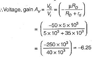
In the CS amplifier shown in figure, if RD = 5 KΩ RG = 10 MΩ, μ = 50, and rd = 35 kΩ.
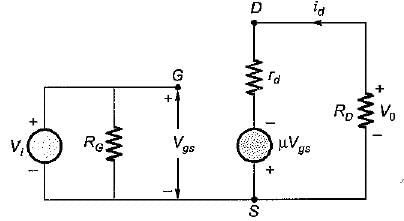
The voltage gain (AV) of the amplifier is

The voltage gain (AV) of the amplifier is
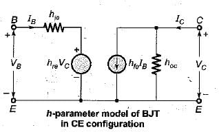
Consider the following statements associated with small signal FET model and A-parameter model of BJT (in CS configuration and CE configuration respectively):
1. Both FET and BJT have a Norton’s output circuit, but the current generated in BJT depends on the input current and not on the input voltage as in FET.
2. There is no feedback from output to input in the FET, whereas a feedback exist in the BJT through the parameter hre.
3. The high input resistance of the FET is replaced by an input resistance of about 1 kΩ for a CE amplifier.
Which of the above statements is/are correct?
1. Both FET and BJT have a Norton’s output circuit, but the current generated in BJT depends on the input current and not on the input voltage as in FET.
2. There is no feedback from output to input in the FET, whereas a feedback exist in the BJT through the parameter hre.
3. The high input resistance of the FET is replaced by an input resistance of about 1 kΩ for a CE amplifier.
Assertion (A): FET is a much more ideal amplifier than the BJT at low frequencies.
Reason (R): FET has high input impedance and there is no feedback from output to input.
Match List-I (Small Signal FET Amplifier Circuits) with List-I I (Voltage Gain) and select the correct answer using the codes given below the lists:
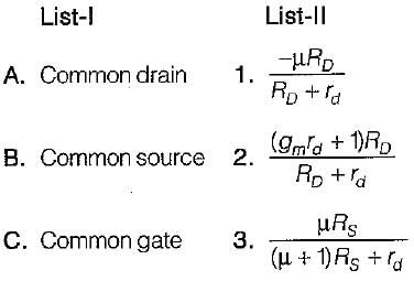
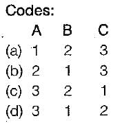
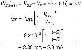
An N-channe! JFET has IDSS = 8 mA and Vp = -5 V. The minimum values of VDS for pinch- off region and the drain current IDS for VGS= - 2V in the pinch-off region are respectively.
Assertion (A): The N-channel MOSFET may turnon prematurely.
Reason (R): The drain resistance of P-channel MOSFET is three times higher than that for an identical N-channei MOSFET
Assertion (A): The input noise is less in N-channel JFET than that in P-channel JFET.
Reason (R): The transconductance of N-channel JFET is smaller than that of P-channel JFET.
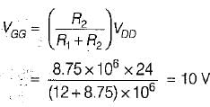
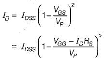
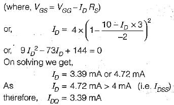
A JFET amplifier with a voltage divider biasing circuit, shown in figure has the following parameters:
Vp = -2 V, IDSS = 4 mA, RD = 910 Ω, Rs =3 kΩ,
R1, = 12 MΩ, R2 = 8.75 MΩ and VDD = 24 V.
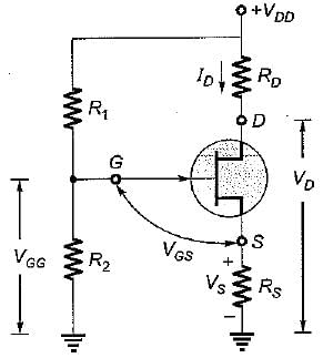
The value of the drain current ID at the operating point is
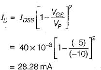
The value of source resistance required to self bias an N-channel JFET with IDSS = 40 mA, Vp = -10 V, VGS = -5 V and VDSQ = 5V is


