Electronics and Communication Engineering (ECE) Exam  >  Electronics and Communication Engineering (ECE) Tests  >  Topicwise Question Bank for Electronics Engineering  >  Test: Realization of Logic Gates - Electronics and Communication Engineering (ECE) MCQ

Test: Realization of Logic Gates - Electronics and Communication Engineering (ECE) MCQ


Test Description

10 Questions MCQ Test Topicwise Question Bank for Electronics Engineering - Test: Realization of Logic Gates
Test: Realization of Logic Gates for Electronics and Communication Engineering (ECE) 2025 is part of Topicwise Question Bank for Electronics Engineering preparation. The Test: Realization of Logic Gates questions and answers have been prepared according to the Electronics and Communication Engineering (ECE) exam syllabus.The Test: Realization of Logic Gates MCQs are made for Electronics and Communication Engineering (ECE) 2025 Exam. Find important definitions, questions, notes, meanings, examples, exercises, MCQs and online tests for Test: Realization of Logic Gates below.
Solutions of Test: Realization of Logic Gates questions in English are available as part of our Topicwise Question Bank for Electronics Engineering for Electronics and Communication Engineering (ECE) & Test: Realization of Logic Gates solutions in Hindi for Topicwise Question Bank for Electronics Engineering course. Download more important topics, notes, lectures and mock test series for Electronics and Communication Engineering (ECE) Exam by signing up for free. Attempt Test: Realization of Logic Gates | 10 questions in 30 minutes | Mock test for Electronics and Communication Engineering (ECE) preparation | Free important questions MCQ to study Topicwise Question Bank for Electronics Engineering for Electronics and Communication Engineering (ECE) Exam | Download free PDF with solutions
Test: Realization of Logic Gates - Question 1

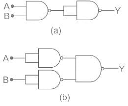
Above are the circuits that consist of NAND gates. Determine the logic operation carried out by these circuits?

Detailed Solution for Test: Realization of Logic Gates - Question 1

Circuit A:

The output X is given as;

The output Y is given as;

Circuit B:

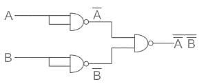
The output P and Q are given as;
P = A̅ 
Q = B̅ 
The output Y is given as;

Test: Realization of Logic Gates - Question 2

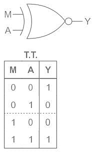
How can we use the X-NOR gate as an inverter?

Detailed Solution for Test: Realization of Logic Gates - Question 2

For two input any gate one of the input can be used as control input and depending on output according to control input the gates can be used for different applications.
Example in XNOR gate, if one of the input is treated as control input, say  M  we observe that if M = 0, output, Y = A̅  means it act as inverter whereas when control input, M = 1, output, Y = A  means output just follow the input.

If control input,
M = 0, Y - A̅ 
If M = 1, Y = A 

Test: Realization of Logic Gates - Question 3

The input to a logic gate is A = 1100 and B = 1010. What will be the output, if the logic gate is NAND gate?

Detailed Solution for Test: Realization of Logic Gates - Question 3

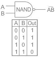
NAND Gate:

  • NAND gate represents the complement of the AND operation.
  • The graphic symbol for the NAND gate consists of an AND symbol with a bubble on the output, denoting that a complement operation is performed on the output of the AND gate. 
  • The logic NAND function can be expressed by the Boolean expression of, A.B.


Analysis:
Given A = 1100 and B = 1010

∴ The output will be 0111.

Test: Realization of Logic Gates - Question 4

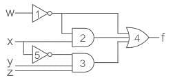
Consider the following gate network:

which gate is redundant

Detailed Solution for Test: Realization of Logic Gates - Question 4


f = x̅ y z + w̅  x + w̅ 
= w̅  (1 + x) + x̅ y z
= w̅ + x̅ y z
∴ As the output of Gate 2 is not coming in the final simplified solution.
Gate 2 Is redundant.

Test: Realization of Logic Gates - Question 5

In the circuit shown in the figure, if C = 0, the expression for Y is

Detailed Solution for Test: Realization of Logic Gates - Question 5

The given circuit is redrawn as:

The output will be:

Test: Realization of Logic Gates - Question 6

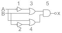
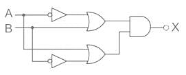
Determine the Boolean function of the following circuit.
Detailed Solution for Test: Realization of Logic Gates - Question 6

Analysis:

Gate 1 is buffer. Input to buffer is A̅ , Output = A̅ 
Gate 2 is buffer. Input to buffer is B̅ , Output = B̅ 
Gate 3 is OR gate. Input = A̅ and B, Output = A̅ + B
Gate 4 is OR gate, Input = A and B̅ , Output = A + B̅ 
Gate 5 is AND gate, Input = (A̅ + B) and (A + B̅), the final output:
x = (A̅ + B) (A + B̅)
x = A̅ B̅ + A B

Test: Realization of Logic Gates - Question 7

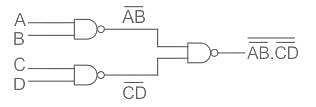
The Boolean function Y = AB + CD is to be realized using only 2 input NAND gates. The minimum number of gates required is

Detailed Solution for Test: Realization of Logic Gates - Question 7

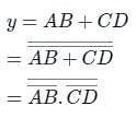
Concept:
De Morgan’s law states that:

Analysis:


Only 3 NAND gates are required

Test: Realization of Logic Gates - Question 8

In an all NOR gate realization of a combinational circuit all EVEN and ODD level gates behave like

Detailed Solution for Test: Realization of Logic Gates - Question 8

In an all NOR gate realization of a combinational circuit,

  • All Even level gates behave like AND gate
  • All Odd level gates behave like OR gate

In an all NAND gate realization of a combinational circuit,

  • All Even level gates behave like OR gate
  • All Odd level gates behave like AND gate
Test: Realization of Logic Gates - Question 9

Consider the logic circuit with input signal TEST shown in the figure. All gates in the figure shown have identical non-zero delay. The signal TEST which was at logic LOW is switched to logic HIGH and maintained at logic HIGH. The output

Detailed Solution for Test: Realization of Logic Gates - Question 9

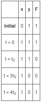
In the given logic circuit, every gate has an identical non-zero delay.
Let the delay is t0 msec.

Initially test signal was at logic LOW.
⇒ x = 0, y = 1

Initially output was HIGH
Let assume test signal is switched to logic high at t = 0 m sec
At, t = 0 m sec, x = 1
As there are three NOT gates, the delay of signal to reach y input is 3t0 msec.
At, t = 3t msec, y = 0 ⇒ remains as before

NAND gate also has delay of t0 msec.
At, t = 4t0 msec, f becomes high.
At, t = 0 msec, x = 1, y = 1
At, t = 100 msec,


Output pulses from HIGH → LOW → HIGH
At, 0 < t < t0, f = HIGH
At, t0 < t < 4t0, f = LOW
At, t = 4t0, f = HIGH

Test: Realization of Logic Gates - Question 10

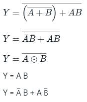
The output equivalent circuit of following circuit is

Detailed Solution for Test: Realization of Logic Gates - Question 10

Concept:
De Morgans law:
The complement of the union of two sets is the intersection of their complements.
(x + y)’ = x’. y’
The complement of the intersection of two sets is the union of their complements.
(x.y)’ = x’ + y’
Analysis:


∴ OR gate

195 tests
Information about Test: Realization of Logic Gates Page
In this test you can find the Exam questions for Test: Realization of Logic Gates solved & explained in the simplest way possible. Besides giving Questions and answers for Test: Realization of Logic Gates, EduRev gives you an ample number of Online tests for practice
Download as PDF