Electrical Engineering (EE) Exam  >  Electrical Engineering (EE) Tests  >  GATE Electrical Engineering (EE) Mock Test Series 2025  >  Test: Logic Families - 1 - Electrical Engineering (EE) MCQ

Test: Logic Families - 1 - Electrical Engineering (EE) MCQ


Test Description

10 Questions MCQ Test GATE Electrical Engineering (EE) Mock Test Series 2025 - Test: Logic Families - 1

Test: Logic Families - 1 for Electrical Engineering (EE) 2025 is part of GATE Electrical Engineering (EE) Mock Test Series 2025 preparation. The Test: Logic Families - 1 questions and answers have been prepared according to the Electrical Engineering (EE) exam syllabus.The Test: Logic Families - 1 MCQs are made for Electrical Engineering (EE) 2025 Exam. Find important definitions, questions, notes, meanings, examples, exercises, MCQs and online tests for Test: Logic Families - 1 below.
Solutions of Test: Logic Families - 1 questions in English are available as part of our GATE Electrical Engineering (EE) Mock Test Series 2025 for Electrical Engineering (EE) & Test: Logic Families - 1 solutions in Hindi for GATE Electrical Engineering (EE) Mock Test Series 2025 course. Download more important topics, notes, lectures and mock test series for Electrical Engineering (EE) Exam by signing up for free. Attempt Test: Logic Families - 1 | 10 questions in 30 minutes | Mock test for Electrical Engineering (EE) preparation | Free important questions MCQ to study GATE Electrical Engineering (EE) Mock Test Series 2025 for Electrical Engineering (EE) Exam | Download free PDF with solutions
Test: Logic Families - 1 - Question 1

As compared to TTL, CMOS logic has

Detailed Solution for Test: Logic Families - 1 - Question 1

Option(1)- Schottky transistors are  preferred for TTL logic systems. These transistors portray the Schottky effect and thus have higher switching speed in comparison to CMOS logic family.So option 1 is false.
Option(2)- TTL dissipates a lot of power where as CMOS uses almost no power in the static state (that is, when inputs are not changing). So option 2  is false.
Option(3)- TTL  requires more space and isolation in comparison to CMOS logic family. The required silicon area for implementing  CMOS  is very small. So option 3 is true.

Test: Logic Families - 1 - Question 2

The figure of merit of a logic family is given by the product of:

Detailed Solution for Test: Logic Families - 1 - Question 2

Figure of merit = Propagation Delay × Power Dissipation
For the best IC operation, FOM should be as small as possible.
Units: ns × mW
= pJ (pico Joule)
Propagation delay (tpd­):


tPHL = delay time in going form High to low logic
tPLH = Delay time in going from low to High logic
Power dissipation (PD):
PD(avg) = Icc × Vcc
VCC = power supply
ICC = avg collector current calculated as the average of the High and low current, i.e.

Test: Logic Families - 1 - Question 3

Two voltage given as -2 V and -1 V in positive logic convention represent:

Detailed Solution for Test: Logic Families - 1 - Question 3

Concept:

The terms positive logic and negative logic refer to two conventions that tell the relationship between logical values and the voltages used to represent them.

  1. Logic 0 is always used to represent false and logic 1 is always used to represent true in Boolean Algebra.
  2. Positive Logic Convention:
    In this, the more positive potential is considered to represent true or logic 1, and the more negative potential is considered to represent false or logic 0.
  3. Negative Logic Convention:
    In this, the more negative potential is considered to represent true or logic 1, and the more positive potential is considered to represent false or logic 0.

Calculation:
Two voltages are given -2 V and -1 V
As we have to represent them in the positive logic convention:
-2 V will represent logic 0 as it is more negative and
-1 V will represent logic 1.
Hence option (3) is the correct answer.

Test: Logic Families - 1 - Question 4

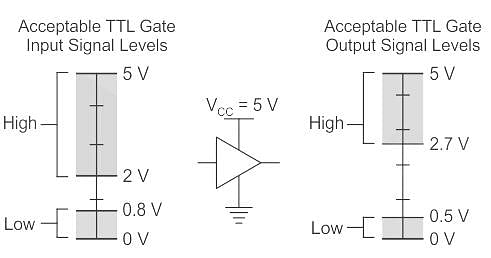
An acceptable voltage range of a logic 0 for TTL

Detailed Solution for Test: Logic Families - 1 - Question 4

TTL (Transistor-Transistor Logic):

  • A TTL input signal is defined as "low" when between 0 V and 0.8 V with respect to the ground terminal. 
  • A TTL input signal is defined as "high" when between 2 V and 5 V.
  • if a voltage signal ranging between 0.8 V and 2.0 V is sent into the input of a TTL gate, there is no certain response from the gate and therefore it is considered "uncertain" (precise logic levels vary slightly between sub-types and by temperature).

  • TTL outputs are typically restricted to narrower limits of between 0.0 V and 0.4 V for a "low".
  • TTL outputs are typically restricted to narrower limits of between 2.4 V and 5 V for a "high", providing at least 0.4 V of noise immunity.
Test: Logic Families - 1 - Question 5

Which of the following statements is incorrect?

Detailed Solution for Test: Logic Families - 1 - Question 5

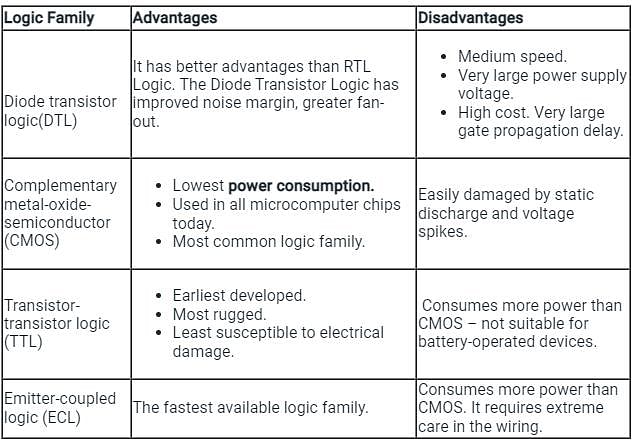
The most important parameters for evaluating and comparing logic families are:

  • Power dissipation
  • Propagation delay
  • Noise margin
  • Fan-out (loading)

General comparison of three commonly available logic families is explained in the following table:


∴ Option 1 is incorrect because the power dissipation in TTL is high and hence CMOS having less waste power as compared to NMOS logic and TTL can be used in highly integrated circuits. 

Test: Logic Families - 1 - Question 6

Which of the following does not belong to TTL subclasses?

Detailed Solution for Test: Logic Families - 1 - Question 6

Transistor-Transistor Logic (TTL):

The Transistor-Transistor Logic (TTL) is a logic family made up of BJTs (bipolar junction transistors).

The TTL family consists of various subfamilies such as standard TTL, low-power TTL, high power TTL, low power Schottky TTL, Schottky TTL, advanced low-power Schottky TTL, advanced Schottky TTL, and fast TTL.

The ICs which belong to the TTL family are designated as follows: 74 or 54 for standard TTL, 74L or 54L for low-power TTL, 74H or 54H for high power TTL, 74ALS or 54ALS for Low power Schottky TTL, and so on.

TTLs are available in different types and their classification is done based on the output like the following.

  • Standard TTL
  • Fast TTL
  • Schottky TTL
  • High Power TTL
  • Low Power TTL
  • Advanced Schottky TTL
Test: Logic Families - 1 - Question 7

A Darlington emitter-follower circuit is sometimes used in the output stage of a TTL gate in order to

Detailed Solution for Test: Logic Families - 1 - Question 7

Concept:

  • In a digital circuit, the Noise Margin is the amount by which the signal exceeds the threshold for a proper ‘0’ or ‘1’.
  • For Ex: a Digital circuit might be designed to swing between 0 and 1.2 Volts, with anything below 0.2 V considered as a ‘0’ and anything above 1 Volt is considered a ‘1’. Then the noise margin for a ‘0’ would be the amount that a signal is below 0.2 Volts, and a noise margin for 1 would be the amount by which a signal exceeds 1 Volt.
  • In this case noise margins are measured as an absolute voltage, not as a ratio.
  • This is schematically explained with the help of the following diagram:


Test: Logic Families - 1 - Question 8

Which logic family dissipates the minimum power?

Detailed Solution for Test: Logic Families - 1 - Question 8

A logic family is one of two related concepts: A logic family of monolithic digital integrated circuit devices is a group of electronic logic gates constructed using one of several different designs, usually with compatible logic levels and power supply characteristics within a family.

Test: Logic Families - 1 - Question 9

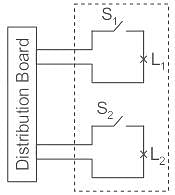
Identify the given wiring diagram of ___________.

Detailed Solution for Test: Logic Families - 1 - Question 9

Joint Box system:

  • In this method of wiring, the connections to appliances are made through joints.
  • These joints are made in joint lines by means of suitable connection or joint cut-outs.
  • This method of wiring doesn’t consume too much cable size.
  • It requires less wiring doesn’t means it is cheaper, although it is cheaper because the amount saved from buying cables will be used in buying joint boxes, thus the equation is balanced.
  • This method is suitable for temporary installation and it is cheap.
  • It is also called ‘Tee system’.

Option 1:
Two lamps controlled by two switches, all connected in series.


Option 2:
Two lamps in series, each having switch in parallel

Option 3:
Two lamps each controlled by a separate switch

Test: Logic Families - 1 - Question 10

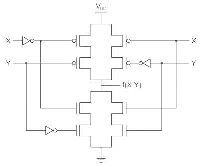
The logic function f(X,Y) realized by the given circuit is
Detailed Solution for Test: Logic Families - 1 - Question 10

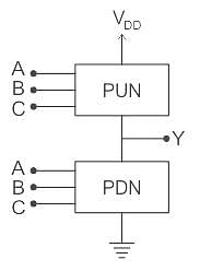
CMOS logic circuit is an extension of a CMOS inverter. It consists of two network transistors, a pull-down network (PDN) constructed of an n-MOS and Pull-up Network (PUN) constructed of P-MOS.

PDN: Since nMOS conducts when the signal gate is high, PDN is activated when the inputs are high.
PUN: It comprises PMOS and conducts when the input signal gate is low.
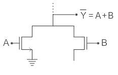
The PDN and PUN are connected in parallel to form OR logic function and they are connected in series to form AND logic as shown:

25 docs|247 tests
Information about Test: Logic Families - 1 Page
In this test you can find the Exam questions for Test: Logic Families - 1 solved & explained in the simplest way possible. Besides giving Questions and answers for Test: Logic Families - 1, EduRev gives you an ample number of Online tests for practice
Download as PDF