Electrical Engineering (EE) Exam  >  Electrical Engineering (EE) Tests  >  GATE Electrical Engineering (EE) Mock Test Series 2025  >  Test: Diode Circuits - 2 - Electrical Engineering (EE) MCQ

Test: Diode Circuits - 2 - Electrical Engineering (EE) MCQ


Test Description

15 Questions MCQ Test GATE Electrical Engineering (EE) Mock Test Series 2025 - Test: Diode Circuits - 2

Test: Diode Circuits - 2 for Electrical Engineering (EE) 2024 is part of GATE Electrical Engineering (EE) Mock Test Series 2025 preparation. The Test: Diode Circuits - 2 questions and answers have been prepared according to the Electrical Engineering (EE) exam syllabus.The Test: Diode Circuits - 2 MCQs are made for Electrical Engineering (EE) 2024 Exam. Find important definitions, questions, notes, meanings, examples, exercises, MCQs and online tests for Test: Diode Circuits - 2 below.
Solutions of Test: Diode Circuits - 2 questions in English are available as part of our GATE Electrical Engineering (EE) Mock Test Series 2025 for Electrical Engineering (EE) & Test: Diode Circuits - 2 solutions in Hindi for GATE Electrical Engineering (EE) Mock Test Series 2025 course. Download more important topics, notes, lectures and mock test series for Electrical Engineering (EE) Exam by signing up for free. Attempt Test: Diode Circuits - 2 | 15 questions in 45 minutes | Mock test for Electrical Engineering (EE) preparation | Free important questions MCQ to study GATE Electrical Engineering (EE) Mock Test Series 2025 for Electrical Engineering (EE) Exam | Download free PDF with solutions
Test: Diode Circuits - 2 - Question 1

In the question a circuit and a waveform for the input voltage is given. The diode in circuit has cutin voltage Vγ = 0. Choose the option for the waveform of output voltage vo :

​ ​ ​

Detailed Solution for Test: Diode Circuits - 2 - Question 1
  • Diode is off for vi  < 5 V. Hence vo = 5 V.
  • For vi > 5 V, vo = vi .Therefore (D) is correct option.
Test: Diode Circuits - 2 - Question 2

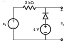
In the question a circuit and a waveform for the input voltage is given. The diode in circuit has cutin voltage Vγ = 0. Choose the option for the waveform of output voltage vo
Detailed Solution for Test: Diode Circuits - 2 - Question 2
  • Diode will be off if vi + 2 > 0.
    Thus vo = 0
  • For v+ 2  < 0 V,
    vi  < -2,
    vo = vi + 2 = -3V
  • Thus (C) is correct option
1 Crore+ students have signed up on EduRev. Have you? Download the App
Test: Diode Circuits - 2 - Question 3

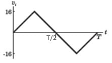
In the question a circuit and a waveform for the input voltage is given. The diode in circuit has cutin voltage Vγ = 0. Choose the option for the waveform of output voltage vo 
Detailed Solution for Test: Diode Circuits - 2 - Question 3
  • For vi  < 4 V the diode is ON and output vo = 4 V.
  • For vi  >4 V diode is off and output vo = vi.
  • Thus (D) is correct option.
Test: Diode Circuits - 2 - Question 4

In the question a circuit and a waveform for the input voltage is given. The diode in circuit has cutin voltage Vγ = 0. Choose the option for the waveform of output voltage vo 

Detailed Solution for Test: Diode Circuits - 2 - Question 4
  • During positive cycle when vs < 8V both diode are OFF vo = vs . For vs > 8V , vo = 8V , D1 is ON.
  • During negative cycle when |vs| < 6 V, both diode are OFF, vo = vs .
  • For |vs| > 6V , D2 is on v0 = -6V .Therefore (C) is correct.
Test: Diode Circuits - 2 - Question 5

For the circuit in fig. P.3.1.5, let cutin voltage Vγ = 0.7 V. The plot of vo verses vi for -10 ≤ vi ≤10 V is:

Detailed Solution for Test: Diode Circuits - 2 - Question 5

Test: Diode Circuits - 2 - Question 6

The circuit inside the box in fig. contains only resistor and diodes. The terminal voltage vo is connected to some point in the circuit inside the box. The largest and smallest possible value of vo most nearly to is respectively.

Detailed Solution for Test: Diode Circuits - 2 - Question 6

The output voltage cannot exceed the positive power supply voltage and cannot be lower than the negative power supply voltage.

Test: Diode Circuits - 2 - Question 7

In the voltage regulator circuit in fig. the maximum load current iL that can be drawn is:

Detailed Solution for Test: Diode Circuits - 2 - Question 7

At regulated power supply:    

will remain less than 1.4 mA.

Test: Diode Circuits - 2 - Question 8

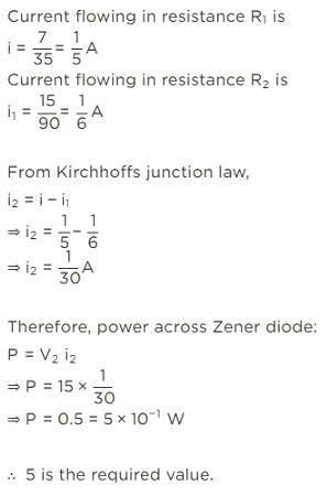
The value of power dissipated across the Zener diode (Vz=15 V) connected in the circuit as shown in the figure is x × 10−1 watts.
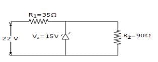
The value of x to the nearest integer is

Detailed Solution for Test: Diode Circuits - 2 - Question 8


Across R1, potential difference is 22 V−15 V = 7 V

Test: Diode Circuits - 2 - Question 9

The Q-point for the Zener diode in fig. is:

Detailed Solution for Test: Diode Circuits - 2 - Question 9

Test: Diode Circuits - 2 - Question 10

In the voltage regulator circuit in fig  the power rating of Zener diode is 400 mW. The value of RL that will establish maximum power in Zener diode is:

Detailed Solution for Test: Diode Circuits - 2 - Question 10

Test: Diode Circuits - 2 - Question 11

In the voltage regulator circuit in fig.  the Zener diode current is to be limited to the range 5 ≤ iz ≤100 mA.

The range of possible load current is:

Detailed Solution for Test: Diode Circuits - 2 - Question 11

Current through 12 Ω resistor is:

Test: Diode Circuits - 2 - Question 12

In the voltage regulator circuit in fig.  the Zener diode current is to be limited to the range 5 ≤ iz ≤100 mA.

The range of possible load resistance is:

Detailed Solution for Test: Diode Circuits - 2 - Question 12

Test: Diode Circuits - 2 - Question 13

In the voltage regulator circuit in fig.  the Zener diode current is to be limited to the range 5 ≤ iz ≤100 mA.

The power rating required for the load resistor is:

Detailed Solution for Test: Diode Circuits - 2 - Question 13

Test: Diode Circuits - 2 - Question 14

The secondary transformer voltage of the rectifier circuit shown in fig. is vs = 60 sin 2π 60tV. Each diode has a cut in voltage of Vγ = 0.6 V. The ripple voltage is to be no more than Vrip = 2 V. The value of filter capacitor will be:

Detailed Solution for Test: Diode Circuits - 2 - Question 14

vs = 60 sin 2π 60tV

Test: Diode Circuits - 2 - Question 15

The input to full-wave rectifier in fig. is vi = 120 sin2π60t V. The diode cutin voltage is 0.7 V. If the output voltage cannot drop below 100 V, the required value of the capacitor is:

Detailed Solution for Test: Diode Circuits - 2 - Question 15

Full wave rectifier:

25 docs|247 tests
Information about Test: Diode Circuits - 2 Page
In this test you can find the Exam questions for Test: Diode Circuits - 2 solved & explained in the simplest way possible. Besides giving Questions and answers for Test: Diode Circuits - 2, EduRev gives you an ample number of Online tests for practice

Top Courses for Electrical Engineering (EE)

Download as PDF

Top Courses for Electrical Engineering (EE)