Electrical Engineering (EE) Exam  >  Electrical Engineering (EE) Tests  >  Test: Electronic Devices & Circuits - 1 - Electrical Engineering (EE) MCQ

Test: Electronic Devices & Circuits - 1 - Electrical Engineering (EE) MCQ


Test Description

25 Questions MCQ Test - Test: Electronic Devices & Circuits - 1

Test: Electronic Devices & Circuits - 1 for Electrical Engineering (EE) 2024 is part of Electrical Engineering (EE) preparation. The Test: Electronic Devices & Circuits - 1 questions and answers have been prepared according to the Electrical Engineering (EE) exam syllabus.The Test: Electronic Devices & Circuits - 1 MCQs are made for Electrical Engineering (EE) 2024 Exam. Find important definitions, questions, notes, meanings, examples, exercises, MCQs and online tests for Test: Electronic Devices & Circuits - 1 below.
Solutions of Test: Electronic Devices & Circuits - 1 questions in English are available as part of our course for Electrical Engineering (EE) & Test: Electronic Devices & Circuits - 1 solutions in Hindi for Electrical Engineering (EE) course. Download more important topics, notes, lectures and mock test series for Electrical Engineering (EE) Exam by signing up for free. Attempt Test: Electronic Devices & Circuits - 1 | 25 questions in 25 minutes | Mock test for Electrical Engineering (EE) preparation | Free important questions MCQ to study for Electrical Engineering (EE) Exam | Download free PDF with solutions
Test: Electronic Devices & Circuits - 1 - Question 1

At room temperature the current in an intrinsic semiconductor is due to

Detailed Solution for Test: Electronic Devices & Circuits - 1 - Question 1

Intrinsic material has equal number of holes and electrons.

Test: Electronic Devices & Circuits - 1 - Question 2

Work function is the maximum energy required by the fastest electron at 0 K to escape from the metal surface.

Detailed Solution for Test: Electronic Devices & Circuits - 1 - Question 2

Work function is the minimum energy required by the fastest electron at 0 K to escape from the metal surface.

1 Crore+ students have signed up on EduRev. Have you? Download the App
Test: Electronic Devices & Circuits - 1 - Question 3

The most commonly used semiconductor material is

Detailed Solution for Test: Electronic Devices & Circuits - 1 - Question 3

Germanium is rarely used.

Test: Electronic Devices & Circuits - 1 - Question 4

In which of these is reverse recovery time nearly zero?

Detailed Solution for Test: Electronic Devices & Circuits - 1 - Question 4

In schottky diode there is no charge storage and hence almost zero reverse recovery time.

Test: Electronic Devices & Circuits - 1 - Question 5

A transistor has a current gain of 0.99 in the CB mode. Its current gain in the CC mode is

Detailed Solution for Test: Electronic Devices & Circuits - 1 - Question 5

Current gain = 1 + β = 100.

Test: Electronic Devices & Circuits - 1 - Question 6

In p-n-p transistor the current IE has two components viz. IEP due to injection of holes from p-region to n-region and IE due to injection of electrons from n-region to p-region. Then

Detailed Solution for Test: Electronic Devices & Circuits - 1 - Question 6

Emitter is p-type in p-n-p transistor.

Therefore holes are majority carriers.

Test: Electronic Devices & Circuits - 1 - Question 7

In an n channel JFET, the gate is

Detailed Solution for Test: Electronic Devices & Circuits - 1 - Question 7

Since channel is n type gate must be p type.

Test: Electronic Devices & Circuits - 1 - Question 8

The amount of photoelectric emission current depends on

Detailed Solution for Test: Electronic Devices & Circuits - 1 - Question 8

Only the intensity of incident radiation governs the amount of photoelectric emission.

Test: Electronic Devices & Circuits - 1 - Question 9

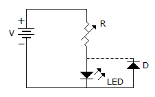
In the circuit of figure the function of resistor R and diode D are
Detailed Solution for Test: Electronic Devices & Circuits - 1 - Question 9

Resistance limits current and diode is reverse connected and therefore protects LED against reverse breakdown.

Test: Electronic Devices & Circuits - 1 - Question 10


Assertion (A): A p-n junction has high resistance in reverse direction.

Reason (R): When a reverse bias is applied to p-n junction, the width of depletion layer increases.


Detailed Solution for Test: Electronic Devices & Circuits - 1 - Question 10

The increase in reverse resistance is due to widening of depletion layer.

Test: Electronic Devices & Circuits - 1 - Question 11

At very high temperatures the extrinsic semi conductors become intrinsic because

Detailed Solution for Test: Electronic Devices & Circuits - 1 - Question 11

Covalent bonds are broken.

Test: Electronic Devices & Circuits - 1 - Question 12

When a voltage is applied to a semiconductor crystal then the free electrons will flow.

Detailed Solution for Test: Electronic Devices & Circuits - 1 - Question 12

Since electrons are negatively charged they will flow towards positive terminal.

Test: Electronic Devices & Circuits - 1 - Question 13

Ferrite have

Detailed Solution for Test: Electronic Devices & Circuits - 1 - Question 13

Ferrite is a low density material of composition with Fe2O3 x O, where x is a bivalent metal, such as Cobart, Ni, Mn. These magnetic materials having very low loss of current and used in high frequency circuit.

Test: Electronic Devices & Circuits - 1 - Question 14

In a p type material the Fermi level is 0.3 eV above valence band. The concentration of acceptor atoms is increased. The new position of Fermi level is likely to be

Detailed Solution for Test: Electronic Devices & Circuits - 1 - Question 14

Addition of acceptor atom brings Fermi level closer to valence band.

Test: Electronic Devices & Circuits - 1 - Question 15

In an n-p-n transistor, the majority carriers in the base are

Detailed Solution for Test: Electronic Devices & Circuits - 1 - Question 15

Emitter is n type and emits electrons which diffuse through the base.

Test: Electronic Devices & Circuits - 1 - Question 16

An LED has a rating of 2 V and 10 mA. It is used along with 6V battery. The range of series resistance is

Detailed Solution for Test: Electronic Devices & Circuits - 1 - Question 16

R = = 400Ω.

R must be at least 400Ω so that current in LED does not exceed 10 mA.

Test: Electronic Devices & Circuits - 1 - Question 17

The number of doped regions in PIN diode is

Detailed Solution for Test: Electronic Devices & Circuits - 1 - Question 17

A PIN diode has p and n doped regions separated by intrinsic layer.

Test: Electronic Devices & Circuits - 1 - Question 18

A transistor has two p-n junctions. The batteries should be connected in active region such that

Detailed Solution for Test: Electronic Devices & Circuits - 1 - Question 18

Emitter-base junction is forward biased and base collector junction is reverse biased.

Test: Electronic Devices & Circuits - 1 - Question 19

A silicon (PN) junction at a temperature of 20ºC has a reverse saturation current of 10 pico Ampere. The reverse saturation current at 40ºC for the same bias is approximately.

Detailed Solution for Test: Electronic Devices & Circuits - 1 - Question 19

By increasing of temperature by 10ºC, Io become double so by increasing temperature 20ºC, Io become 4 time than initial value... and it is 40 PA.

Test: Electronic Devices & Circuits - 1 - Question 20

In a bipolar transistor the barrier potential

Detailed Solution for Test: Electronic Devices & Circuits - 1 - Question 20

Since there are two p-n junctions, there are two depletion layers and 0.7 V across each layer.

Test: Electronic Devices & Circuits - 1 - Question 21

Recombination produces new electron-hole pairs

Detailed Solution for Test: Electronic Devices & Circuits - 1 - Question 21

Due to recombination the number of electron-hole pairs is reduced.

Test: Electronic Devices & Circuits - 1 - Question 22

An amplifier without feedback has a voltage gain of 50, input resistance of 1 kΩ and output resistance of 2.5 kΩ. The input resistance of the current shunt -ve feedback amplifier using the above amplifier with a feedback factor of 0.2 is

Detailed Solution for Test: Electronic Devices & Circuits - 1 - Question 22

Input Resistance with feedback for current shunt, .

Test: Electronic Devices & Circuits - 1 - Question 23

As compared to an ordinary semiconductor diode, a Schottky diode

Detailed Solution for Test: Electronic Devices & Circuits - 1 - Question 23

Cut in voltage in Schottky diode is about 0.3 V as compared to 0.7 V in ordinary semiconductor diode.

Test: Electronic Devices & Circuits - 1 - Question 24

Assertion (A): When a high reverse voltage is applied to a p-n junction the diode breaks down.

Reason (R): High reverse voltage causes Avalanche effect.

Detailed Solution for Test: Electronic Devices & Circuits - 1 - Question 24

Avalanche breakdown occurs at high reverse voltage.

Test: Electronic Devices & Circuits - 1 - Question 25

As compared to an ordinary semiconductor diode, a Schottky diode

Detailed Solution for Test: Electronic Devices & Circuits - 1 - Question 25

This is due to high electron concentration in metals.

Information about Test: Electronic Devices & Circuits - 1 Page
In this test you can find the Exam questions for Test: Electronic Devices & Circuits - 1 solved & explained in the simplest way possible. Besides giving Questions and answers for Test: Electronic Devices & Circuits - 1, EduRev gives you an ample number of Online tests for practice

Top Courses for Electrical Engineering (EE)

Download as PDF

Top Courses for Electrical Engineering (EE)