Electrical Engineering (EE) Exam  >  Electrical Engineering (EE) Tests  >  Test: Electronic Devices & Circuits - 2 - Electrical Engineering (EE) MCQ

Test: Electronic Devices & Circuits - 2 - Electrical Engineering (EE) MCQ


Test Description

25 Questions MCQ Test - Test: Electronic Devices & Circuits - 2

Test: Electronic Devices & Circuits - 2 for Electrical Engineering (EE) 2024 is part of Electrical Engineering (EE) preparation. The Test: Electronic Devices & Circuits - 2 questions and answers have been prepared according to the Electrical Engineering (EE) exam syllabus.The Test: Electronic Devices & Circuits - 2 MCQs are made for Electrical Engineering (EE) 2024 Exam. Find important definitions, questions, notes, meanings, examples, exercises, MCQs and online tests for Test: Electronic Devices & Circuits - 2 below.
Solutions of Test: Electronic Devices & Circuits - 2 questions in English are available as part of our course for Electrical Engineering (EE) & Test: Electronic Devices & Circuits - 2 solutions in Hindi for Electrical Engineering (EE) course. Download more important topics, notes, lectures and mock test series for Electrical Engineering (EE) Exam by signing up for free. Attempt Test: Electronic Devices & Circuits - 2 | 25 questions in 25 minutes | Mock test for Electrical Engineering (EE) preparation | Free important questions MCQ to study for Electrical Engineering (EE) Exam | Download free PDF with solutions
Test: Electronic Devices & Circuits - 2 - Question 1

An incremental model of a solid state device is one which represents the

Detailed Solution for Test: Electronic Devices & Circuits - 2 - Question 1

Incremental model is used for ac response at one operating point.

Test: Electronic Devices & Circuits - 2 - Question 2

What is the correct sequence of the following step in the fabrication of a monolithic, Bipolar junction transistor?

  1. Emitter diffusion
  2. Base diffusion
  3. Buried layer formation
  4. E pi-layer formation
Select the correct answer using the codes given below:

Detailed Solution for Test: Electronic Devices & Circuits - 2 - Question 2

It is always non-linear.

1 Crore+ students have signed up on EduRev. Have you? Download the App
Test: Electronic Devices & Circuits - 2 - Question 3

For an n-channel enhancement type MOSFET, if the source is connected at a higher potential than that of the bulk (VSB > 0), the threshold voltage VT of the MOSFET will

Detailed Solution for Test: Electronic Devices & Circuits - 2 - Question 3

VT depends upon MOSFET construction, hence it will Independent from MOSFET parameters.

Test: Electronic Devices & Circuits - 2 - Question 4

Which of the following is used for generating time varying wave forms?

Detailed Solution for Test: Electronic Devices & Circuits - 2 - Question 4

Its output is used to trigger SCR.

Test: Electronic Devices & Circuits - 2 - Question 5

Calculate the resistivity of n-type semiconductor from the following data, Density of holes = 5 x 1012 cm-3. Density of electrons = 8 x 1013 cm-3, mobility of conduction electron = 2.3 x 104 cm2/ V-sec and mobility of holes = 100 cm2/V-sec.

Detailed Solution for Test: Electronic Devices & Circuits - 2 - Question 5

Resistivity(r) = .

σ = e(neue + nnun).

Test: Electronic Devices & Circuits - 2 - Question 6

An one sided abrupt junction has 1021/m3 of dopants on the lightly doped side, zero bias voltage and a built-in potential of 0.2 V. The depletion width of abrupt junction.(q = 1.6 x 10⁻¹⁹ C, εr =16, ε0 = 8.87 x 10⁻¹² F/m) is

Detailed Solution for Test: Electronic Devices & Circuits - 2 - Question 6

.

Test: Electronic Devices & Circuits - 2 - Question 7

n-type semiconductors

Detailed Solution for Test: Electronic Devices & Circuits - 2 - Question 7

n type semiconductor is produced when pentavalent impurity is added.

Test: Electronic Devices & Circuits - 2 - Question 8

In all metals

Detailed Solution for Test: Electronic Devices & Circuits - 2 - Question 8

In all metals conductivity decreases (and resistance increases) with increase in temperature.

Test: Electronic Devices & Circuits - 2 - Question 9

The voltage across a zener diode

Detailed Solution for Test: Electronic Devices & Circuits - 2 - Question 9

Zener diode is always reverse biased.

Test: Electronic Devices & Circuits - 2 - Question 10

Assertion (A): Two transistors one n-p-n and the other p-n-p are identical in all respects (doping, construction, shape, size). The n-p-n transistor will have better frequency response.

Reason (R): The electron mobility is higher than hole mobility.

Detailed Solution for Test: Electronic Devices & Circuits - 2 - Question 10

Therefore mostly npn transistors are used.

Test: Electronic Devices & Circuits - 2 - Question 11

The threshold voltage of an n-channel enhancement mode MOSFET is 0.5 when the device is biased at a gate voltage of 3V. Pinch off would occur at a drain voltage of

Detailed Solution for Test: Electronic Devices & Circuits - 2 - Question 11

It is used with reverse bias.

Test: Electronic Devices & Circuits - 2 - Question 12

Which of these has degenerate p and n materials?

Detailed Solution for Test: Electronic Devices & Circuits - 2 - Question 12

Tunnel diode has heavily doped p and n layers called degenerate p and n materials.

Test: Electronic Devices & Circuits - 2 - Question 13

A Schottky diode clamp is used along with switching BJT for

Detailed Solution for Test: Electronic Devices & Circuits - 2 - Question 13

Schottky diode has very low switching time.

Test: Electronic Devices & Circuits - 2 - Question 14

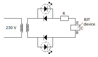
From the given circuit below, we can conclude that.
Detailed Solution for Test: Electronic Devices & Circuits - 2 - Question 14

According to figure, both the LED is glowing, which indicate that circuit is complete in both the half cycle of a.c. signal.

Therefore Emitter and Base junction will act as short circuit in both direction, which indicate transistor is faulty.

Test: Electronic Devices & Circuits - 2 - Question 15

In a piezoelectric crystal, applications of a mechanical stress would produce

Detailed Solution for Test: Electronic Devices & Circuits - 2 - Question 15

In piezoelectric materials mechanical stress produces electric polarization.

Test: Electronic Devices & Circuits - 2 - Question 16

In which of the following is the width of junction barrier very small?

Detailed Solution for Test: Electronic Devices & Circuits - 2 - Question 16

Schottky diode has very small depletion layer.

Test: Electronic Devices & Circuits - 2 - Question 17

If the reverse voltage across a p-n junction is increased three times, the junction capacitance

Detailed Solution for Test: Electronic Devices & Circuits - 2 - Question 17

Increase of reverse voltage widens the depletion layer and junction capacitance decreases. However the decrease in capacitance is not proportional to increase in voltage.

Test: Electronic Devices & Circuits - 2 - Question 18

Which of these has highly doped p and n region?

Detailed Solution for Test: Electronic Devices & Circuits - 2 - Question 18

Tunnel diode has heavily doped p and n regions leading to very thin depletion layer.

Test: Electronic Devices & Circuits - 2 - Question 19

Measurement of Hall coefficient enables the determination of

Detailed Solution for Test: Electronic Devices & Circuits - 2 - Question 19

If a potential difference is developed across a current carrying metal strip when the strip is placed in transverse magnetic field.

Hall effect is very weak in metals, but it is large semiconductors.

Test: Electronic Devices & Circuits - 2 - Question 20

The units for transconductance are

Detailed Solution for Test: Electronic Devices & Circuits - 2 - Question 20

Its units are the same as the units of conductance.

Test: Electronic Devices & Circuits - 2 - Question 21

The amount of photoelectric emission current depends on the frequency of incident light.

Detailed Solution for Test: Electronic Devices & Circuits - 2 - Question 21

It depends on intensity of incident light.

Test: Electronic Devices & Circuits - 2 - Question 22

When a p-n junction is forward biased

Detailed Solution for Test: Electronic Devices & Circuits - 2 - Question 22

Forward voltage decreases the width of depletion layer leading to low resistance.

Test: Electronic Devices & Circuits - 2 - Question 23

The carriers of n channel JFET are

Detailed Solution for Test: Electronic Devices & Circuits - 2 - Question 23

In n type semiconductors carriers are electrons.

Test: Electronic Devices & Circuits - 2 - Question 24

The depletion layer around p-n junction in JFET consists of

Detailed Solution for Test: Electronic Devices & Circuits - 2 - Question 24

Depletion layer always has immobile charges.

Test: Electronic Devices & Circuits - 2 - Question 25

Junction temperature is always the same as room temperature.

Detailed Solution for Test: Electronic Devices & Circuits - 2 - Question 25

When the device is being used, junction temperature is higher than room temperature.

Information about Test: Electronic Devices & Circuits - 2 Page
In this test you can find the Exam questions for Test: Electronic Devices & Circuits - 2 solved & explained in the simplest way possible. Besides giving Questions and answers for Test: Electronic Devices & Circuits - 2, EduRev gives you an ample number of Online tests for practice

Top Courses for Electrical Engineering (EE)

Download as PDF

Top Courses for Electrical Engineering (EE)