Electronics and Communication Engineering (ECE) Exam  >  Electronics and Communication Engineering (ECE) Tests  >  Analog Circuits  >  Test: Limits of Operation - Electronics and Communication Engineering (ECE) MCQ

Test: Limits of Operation - Electronics and Communication Engineering (ECE) MCQ


Test Description

10 Questions MCQ Test Analog Circuits - Test: Limits of Operation

Test: Limits of Operation for Electronics and Communication Engineering (ECE) 2025 is part of Analog Circuits preparation. The Test: Limits of Operation questions and answers have been prepared according to the Electronics and Communication Engineering (ECE) exam syllabus.The Test: Limits of Operation MCQs are made for Electronics and Communication Engineering (ECE) 2025 Exam. Find important definitions, questions, notes, meanings, examples, exercises, MCQs and online tests for Test: Limits of Operation below.
Solutions of Test: Limits of Operation questions in English are available as part of our Analog Circuits for Electronics and Communication Engineering (ECE) & Test: Limits of Operation solutions in Hindi for Analog Circuits course. Download more important topics, notes, lectures and mock test series for Electronics and Communication Engineering (ECE) Exam by signing up for free. Attempt Test: Limits of Operation | 10 questions in 10 minutes | Mock test for Electronics and Communication Engineering (ECE) preparation | Free important questions MCQ to study Analog Circuits for Electronics and Communication Engineering (ECE) Exam | Download free PDF with solutions
Test: Limits of Operation - Question 1

For a BJT, what is typically the shape of the power dissipation curve, if it’s plotted on the output characterisics?

Detailed Solution for Test: Limits of Operation - Question 1

Power Dissipation in a BJT is given by P=VCE.IC. This is in the form of k=xy which is the equation of a hyperbola.

Test: Limits of Operation - Question 2

What is the region on the output characteristics below IC = ICEO line called?

Detailed Solution for Test: Limits of Operation - Question 2

The region below IC = ICEO is called the cutoff region.

Test: Limits of Operation - Question 3

What is the region on the output characteristics for VCE < VCEsat called?

Detailed Solution for Test: Limits of Operation - Question 3

The region below VCE < VCEsat is called the saturation region.

Test: Limits of Operation - Question 4

In a BJT amplifier the power gain from base to collector is 4000. The power gain in dB is

Detailed Solution for Test: Limits of Operation - Question 4

Gain in dB = 10 log (4000).

Test: Limits of Operation - Question 5

Given that the collector power dissipation is 300 mW, what is the value of collector current for the collector to emitter voltage = 12 V?

Detailed Solution for Test: Limits of Operation - Question 5

 P=VCE.IC => 300mW = (12V)IC => IC=300/12 mA = 25 mA.

Test: Limits of Operation - Question 6

 Given that the collector power dissipation is 300 mW, what is the value of collector to emitter voltage for collector current = 50 mA?

Detailed Solution for Test: Limits of Operation - Question 6

 P=VCE.IC => 300mW = VCE(50 mA) => VCE = 300/50 = 6 V.

Test: Limits of Operation - Question 7

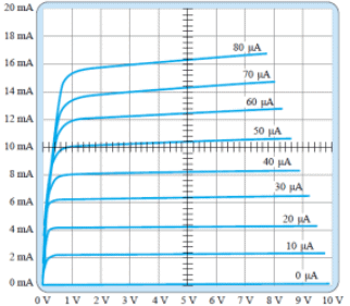
From the given curve tracer response, what is the value of β for IC = 7 mA and VCE = 5 V?

Detailed Solution for Test: Limits of Operation - Question 7

From the curve, we get change in IC = (8.2-6.4) mA and change in IB = 10 uA. Hence, /beta; = (1.8/0.01) = 180.

Test: Limits of Operation - Question 8

If the positive lead of a DMM, with the mode set to ohmmeter is connected to the base and the negative lead to the emitter and a low resistance reading is obtained, then what is the type of transistor that is being tested?

Detailed Solution for Test: Limits of Operation - Question 8

If the positive lead of a DMM, with the mode set to ohmmeter is connected to the base and the negative lead to the emitter and a low resistance reading is obtained, then what is the type of transistor that is being tested is npn.

Test: Limits of Operation - Question 9

If the positive lead of a DMM, with the mode set to ohmmeter is connected to the base and the negative lead to the emitter and a high resistance reading is obtained, then what is the type of transistor that is being tested?

Detailed Solution for Test: Limits of Operation - Question 9

When testing a transistor using a Digital Multimeter (DMM) set to the ohmmeter (resistance) mode, the readings can help identify the type of transistor based on the behavior of its internal junctions. Let's analyze the scenario step-by-step.

Given Scenario:

  • Connections:
    • Positive Lead (Red) of the DMM is connected to the Base.
    • Negative Lead (Black) of the DMM is connected to the Emitter.
  • Observation: A high resistance reading is obtained.

Understanding Transistor Types:

Transistors primarily come in two types:

  1. NPN Transistor
  2. PNP Transistor

Each type has different configurations of p-type and n-type semiconductor materials:

  • NPN Transistor:
    • Structure: Emitter (n-type) → Base (p-type) → Collector (n-type)
    • Base-Emitter Junction: p-n junction
  • PNP Transistor:
    • Structure: Emitter (p-type) → Base (n-type) → Collector (p-type)
    • Base-Emitter Junction: n-p junction

Behavior During Testing:

  1. Testing an NPN Transistor:

    • Connection: Positive (Red) to Base (p-type), Negative (Black) to Emitter (n-type)
    • Result: This forward biases the base-emitter junction (like a forward-biased diode), allowing current to flow.
    • DMM Reading: Low resistance
  2. Testing a PNP Transistor:

    • Connection: Positive (Red) to Base (n-type), Negative (Black) to Emitter (p-type)
    • Result: This reverse biases the base-emitter junction (like a reverse-biased diode), preventing current flow.
    • DMM Reading: High resistance

Applying to the Given Scenario:

  • Observation: High resistance is obtained when the positive lead is connected to the base and the negative lead to the emitter.
  • Inference: Since a high resistance reading indicates that the base-emitter junction is reverse biased, it aligns with the behavior of a PNP transistor under these connections.

Conclusion:

Based on the high resistance reading when the positive lead is connected to the base and the negative lead to the emitter, the transistor being tested is a PNP transistor.

Answer:
a) pnp

Test: Limits of Operation - Question 10

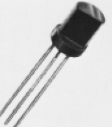
For the given transistor, what is the correct sequence of the pins from left to right?

Detailed Solution for Test: Limits of Operation - Question 10

 With the curved side facing away the correct lead sequence is base, collector, emitter.

3 videos|34 docs|64 tests
Information about Test: Limits of Operation Page
In this test you can find the Exam questions for Test: Limits of Operation solved & explained in the simplest way possible. Besides giving Questions and answers for Test: Limits of Operation, EduRev gives you an ample number of Online tests for practice
3 videos|34 docs|64 tests
Download as PDF