Test: Microprocessor & Digital Logic Families - Electrical Engineering (EE) MCQ
15 Questions MCQ Test - Test: Microprocessor & Digital Logic Families

Consider the following program of 8085 assembly language:
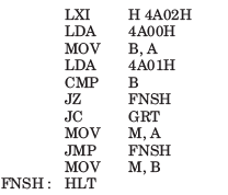
If the contents of memory location 4A00H, 4A01H and 4A02H, are respectively A7H, 98H and 47H, then after the execution of program contents of memory location 4A02H will be respectively
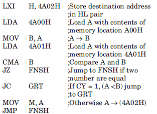
Consider the following program of 8085 assembly language:
Que: The memory requirement for this program is

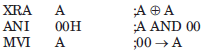
The instruction, that does not clear the accumulator of 8085, is
Consider the following loop
XRA A
LXI B, 0007H
LOOP : DCX B
JNZ LOOP
This loop will be executed
How many address bits are needed to select all memory locations in the 2118 16K × 1 RAM?
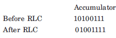
The contents of accumulator after the execution of following instruction will be
MVI A, A7H
ORA A
RLC
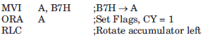
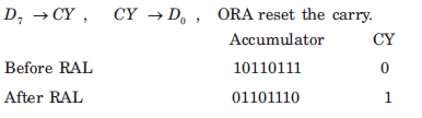
The contents of accumulator after the execution of following instructions will be
MVI A, B7H
ORA A
RAL
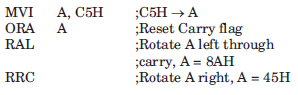
The contents of the accumulator after the execution of the following program will be
MVI A, C5H
ORA A
RAL
Consider the following set of instruction
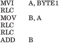
If BYTE1 = 07H, then content of A, after the execution of program will be
Consider the following program
MVI A,BYTE1
RRC
RRC
If BYTE1 = 32H, the contents of A after the execution of program will be
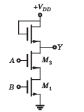
The circuit shown in fig. acts as a
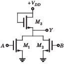
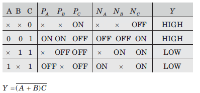
The circuit shown in fig. implements the function
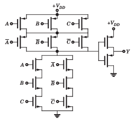

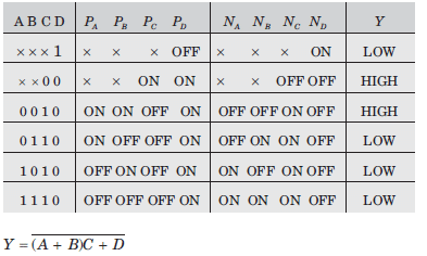
The circuit shown in fig. implements the function
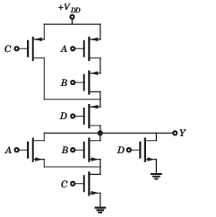
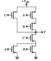
Consider the CMOS circuit shown in fig. The output Y is


Important Questions for Microprocessor & Digital Logic Families
Microprocessor & Digital Logic Families MCQs with Answers
Online Tests for Microprocessor & Digital Logic Families
|
© EduRev
|
Education Revolution
|


|


