NEET Exam  >  NEET Test  >  Physics Class 12  >  Test: Semiconductor Electronics - NEET MCQ

Semiconductor Electronics - Free MCQ Practice Test with solutions, NEET


MCQ Practice Test & Solutions: Test: Semiconductor Electronics (25 Questions)

You can prepare effectively for NEET Physics Class 12 with this dedicated MCQ Practice Test (available with solutions) on the important topic of "Test: Semiconductor Electronics ". These 25 questions have been designed by the experts with the latest curriculum of NEET 2026, to help you master the concept.

Test Highlights:

  • - Format: Multiple Choice Questions (MCQ)
  • - Duration: 25 minutes
  • - Number of Questions: 25

Sign up on EduRev for free to attempt this test and track your preparation progress.

Test: Semiconductor Electronics - Question 1

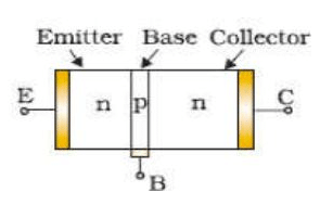
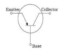
Basic materials used in the present solid state electronic devices like diode, transistor, ICs, etc are

Detailed Solution: Question 1

Explanation:Semiconductors are materials that have electrical conductivity between conductors such as most metals and nonconductors or insulators like ceramics. Semiconductor material is used in the manufacturing of electrical components and used in electronic devices such as transistors and diodes.Semiconductors are the basic materials used in the present solid state electronic devices like diode, transistor, ICs etc

Test: Semiconductor Electronics - Question 2

Depletion region (space charge) is formed because

Detailed Solution: Question 2

Explanation:The depletion region, also called depletion layer, depletion zone, junction region, space charge region or space charge layer, is an insulating region within a conductive, doped semiconductor material where the mobile charge carriers have been diffused away, or have been forced away by an electric field. The only elements left in the depletion region are ionized donor or acceptor impurities.The depletion region is so named because it is formed from a conducting region by removal of all free charge carriers, leaving none to carry a current.

Test: Semiconductor Electronics - Question 3

The conductivity of P – type semiconductor is due to

Detailed Solution: Question 3

A P-type semiconductor is formed when a trivalent electron deficient impurities such as boron group elements are doped with intrinsic semiconductor. As the impurities are electron deficient, they take electrons from the valence band creating a number of holes. Due this reason conductivity in P-type semiconductor is mainly due to holes rather than electrons.

Test: Semiconductor Electronics - Question 4

In an N-P-N transistor, P-type crystal is

Detailed Solution: Question 4

Explanation:When the p-type crystal is grown between relatively wide sections of n-type crystals then the transistor is called NPN transistor.


Test: Semiconductor Electronics - Question 5

In the case of metals the valence and conduction bands have

Detailed Solution: Question 5

Explanation:The materials can be classified by the energy gap between their valence band and the conduction band. The valence band is the band consisting of the valence electron, and the conduction band remains empty. Conduction takes place when an electron jumps from valence band to conduction band and the gap between these two bands is forbidden energy gap. Wider the gap between the valence and conduction bands, higher the energy it requires for shifting an electron from valence band to the conduction band.In the case of conductors, this energy gap is absent or in other words conduction band, and valence band overlaps each other. Thus, electron requires minimum energy to jump from valence band. The typical examples of conductors are Silver, Copper, and Aluminium.In insulators, this gap is vast. Therefore, it requires a significant amount of energy to shift an electron from valence to conduction band. Thus, insulators are poor conductors of electricity. Mica and Ceramic are the well-known examples of insulation material.Semiconductors, on the other hand, have an energy gap which is in between that of conductors and insulators. This gap is typically more or less 1 eV, and thus, one electron requires energy more than conductors but less than insulators for shifting valence band to conduction band.

Test: Semiconductor Electronics - Question 6

In a p-n junction, as the diffusion process continues the width of the depletion zone

Detailed Solution: Question 6

In reverse biasing, the positive terminal of the battery is connected to the n-type whereas the negative terminal is connected to the p-type junction. So the positive terminal tends to pull the electrons (near to the depletion layer) in n-type towards itself whereas the negative terminal pulls the holes towards itself which results in an increase in the width of the depletion layer.

Test: Semiconductor Electronics - Question 7

An N-type Ge is obtained on doping the Ge- crystal with

Detailed Solution: Question 7

Explanation:The addition of pentavalent impurities such as antimony, arsenic or phosphorous contributes free electrons, greatly increasing the conductivity of the intrinsic semiconductor.

Test: Semiconductor Electronics - Question 8

A p- type semiconductor can be obtained by adding

Detailed Solution: Question 8

Explanation:In P-type doping, boron or gallium is the dopant. Boron and gallium each have only three outer electrons. When mixed into the silicon lattice, they form "holes" in the lattice where a silicon electron has nothing to bond to. The absence of an electron creates the effect of a positive charge, hence the name P-type.Holes can conduct current. A hole happily accepts an electron from a neighbor, moving the hole over a space. P-type silicon is a good conductor.

Test: Semiconductor Electronics - Question 9

In a semiconductor crystal, if current flows due to breakage of crystal bonds, then the semiconductor is called

Detailed Solution: Question 9

In the case of an intrinsic semiconductor (say Si) where each Si is having 4 outermost electrons, its crystal structure consists of making 4 covalent bonds with 4 neighbouring Si atoms. Each bond consists of two electrons.

Now if one of the bonds gets broken due to some reason (collisions or high temperature) then one electron gets free and it will be having sufficient energy to cross the band gap and be ready for conduction- So in intrinsic semiconductors, current flows due to breakage of crystal bonds.
 

Test: Semiconductor Electronics - Question 10

Which of the following is not a semiconductor?

Detailed Solution: Question 10

Explanation:Materials that have the resistance levels between those of a conductor and an insulator are referred to as semiconductors.They are quite common, found in almost all electronic devices. Good examples of semiconductor materials are germanium, selenium, and silicon.Radium is a chemical element with symbol Ra and atomic number 88. It is the sixth element in group 2 of the periodic table, also known as the alkaline earth metals.

Test: Semiconductor Electronics - Question 11

Majority current carriers in N – types are

Detailed Solution: Question 11

Explanation:The more abundant charge carriers are called majority carriers, which are primarily responsible for current transport in a piece of semiconductor. In n-type semiconductors they are electrons, while in p-type semiconductors they are holes.

Test: Semiconductor Electronics - Question 12

The depletion layer in the p-n junction is caused

Detailed Solution: Question 12

When a p−n junction is formed, some of the free electrons in the n region diffuse across the junction and combine with holes to form negative ions. In doing so they leave behind positive ions at the donor impurity sites. Similarly, holes from p side diffuse to the n side and thus form a layer called diffusion layer at the junction.
So the depletion region is caused by the diffusion of charge carriers.
 

Test: Semiconductor Electronics - Question 13

When n –type of semiconductor is heated

Detailed Solution: Question 13

Explanation:Due to heating, when a free electron is produced then simultaneously a hole is also produced.

Test: Semiconductor Electronics - Question 14

In a pure, or intrinsic, semiconductor, valence band holes and conduction-band electrons are always present

Detailed Solution: Question 14

Explanation:An intrinsic semiconductor, also called an undoped semiconductor or i-type semiconductor, is a pure semiconductor without any significant dopant species present. The number of charge carriers is therefore determined by the properties of the material itself instead of the amount of impurities. In intrinsic semiconductors the number of excited electrons and the number of holes are equal: n = p.

Test: Semiconductor Electronics - Question 15

In a semiconductor, the forbidden energy gap between the valance band and the conduction band is of the order of

Detailed Solution: Question 15

Explanation:The material which has electrical conductivity between that of a conductor and an insulator is called as semiconductor. Silicon, germanium and graphite are some examples of semiconductors.


In semiconductors, the forbidden gap between valence band and conduction band is very small. It has a forbidden gap of about 1 electron volt (eV).

Test: Semiconductor Electronics - Question 16

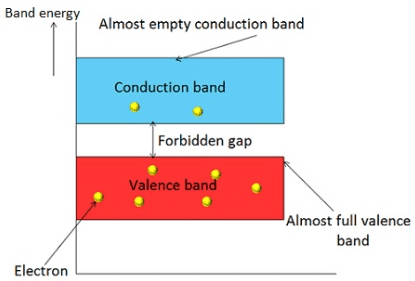
A solid having uppermost energy – band partially filled with electrons is called

Detailed Solution: Question 16

Conductor is an object or type of material that allows the flow of an electrical current in one more directions. A metal wire is a common electrical conductor. In metals such as copper or aluminium, the mobile charged particles are welcome.

Test: Semiconductor Electronics - Question 17

Doping of semiconductor is the process of

Detailed Solution: Question 17

Explanation:Doping is the process of adding impurities to intrinsic semiconductors to alter their properties. Normally Trivalent and Pentavalent elements are used to dope Silicon and Germanium. When an intrinsic semiconductor is doped with Trivalent impurity it becomes a P-Type semiconductor.

Test: Semiconductor Electronics - Question 18

Hole is

Detailed Solution: Question 18

Concept of holes in the semiconductor:

  1. When an electron is removed from a covalent bond, it leaves a vacancy behind. An electron from a neighbouring atom can move into this vacancy, leaving the neighbour with a vacancy. In this way the vacancy formed is called a hole (or cotter), and can travel through the material and serve as an additional current carriers.
  2. A hole is considered as a seat of positive charge, having magnitude of charge equal to that of an electron.
  3. Holes acts as a virtual charge, although there is no physical charge on it.
  4. Effective mass of hole is more than an electron.
  5. Mobility of hole is less than an electron.

Test: Semiconductor Electronics - Question 19

When a P- N junction is reversed biased, the flow of current across the junction is mainly due to

Detailed Solution: Question 19

When p-n junction is reverse biased, the flow of current is due to drifting of minority charge carriers across the junction.

Test: Semiconductor Electronics - Question 20

The main difference between conductors, semiconductors and insulators is because of

Detailed Solution: Question 20

Explanation:Forbidden gap plays a major role for determining the electrical conductivity of material. Based on the forbidden gap materials are classified in to three types, they are : Insulators : The forbidden gap between the valence band and conduction band is very large in insulators. The energy gap of insulator is approximately equal to 15 electron volts (eV).Conductors: In a conductor, valence band and conduction band overlap each other. Therefore, there is no forbidden gap in a conductor.Semiconductors: In semiconductors, the forbidden gap between valence band and conduction band is very small. It has a forbidden gap of about 1 electron volt (eV).

Test: Semiconductor Electronics - Question 21

In the middle of the depletion layer of a reverse biased p-n-junction, the

Detailed Solution: Question 21

Due to the reverse biasing, the width of the depletion region increases and current flowing through the diode is almost zero. In this case, electric field is almost zero at the middle of the depletion region.

Test: Semiconductor Electronics - Question 22

Motion of hole is a convenient way of describing

Detailed Solution: Question 22

Explanation:The holes are just the abscence of a electron in a energy band. But its easier to describe the abscence of a electron as a single moving positive charge than it is to describe the motion of all the other electrons in the band.In a band you have N electrons. Remove one of those electrons(by for instance p-doping) and you have N-1 electrons left. Now you can either choose to describe this with the behavior of those N-1 electrons. Or you can choose to describe it as if there is one single hole moving around in the band.So mathematicly the holes behave just like a positivly charged electron.

Test: Semiconductor Electronics - Question 23

When the conductivity of a semiconductor is only due to breaking of the covalent bonds, the semiconductor is called

Detailed Solution: Question 23

Explanation:A pure semiconductor is called intrinsic semiconductor, e.g., silicon, germanium. The presence of the mobile charge carriers is the intrinsic property of the material. At room temperature, some covalent bonds are broken and electrons are made free. The absence of electron in the covalent bond form hole.The electrical conduction is by means of mobile electrons and holes. Hole act as positive charge, because it can attract an electron. If some other bond is broken and the electron thus freed fills this hole(vacancy), it seems as though the hole is moving.Actually an electron is travelling in opposite direction. In a pure(intrinsic) semiconductor, the number of holes is equal to the number of free electrons.

Test: Semiconductor Electronics - Question 24

The difference in variation of resistance with temperature in a metal and semiconductor is due to

Detailed Solution: Question 24

In metals, scattering increases with temperature and hence the flow of electrons is restricted. In semiconductors, the number of charge carriers increases with temperature which overcomes the effect of increasing scattering and hence the resistivity of semiconductors decreases with an increase in temperature but that of metals increases.

Test: Semiconductor Electronics - Question 25

A piece of copper and another of germanium are cooled from room temperature to 80 K. The resistance of

Detailed Solution: Question 25

We know, a piece of copper is a metal while that of germanium is a semiconducting material. For metals resistance increases with increase in temperature. The semiconductor has a negative temperature coefficient of resistance. Hence, when it is cooled its resistance increases.

74 videos|347 docs|82 tests
Information about Test: Semiconductor Electronics Page
In this test you can find the Exam questions for Test: Semiconductor Electronics solved & explained in the simplest way possible. Besides giving Questions and answers for Test: Semiconductor Electronics , EduRev gives you an ample number of Online tests for practice
74 videos|347 docs|82 tests
Download as PDF