Test: Semiconductors - 6 - JEE MCQ
19 Questions MCQ Test - Test: Semiconductors - 6
In pure silicon at 300 K the electron and hole concentration is each equal to 1.5 × 10¹⁶ m−3. When doped with indium, the hole concentration increases to 4.5 × 10²² m−3. What is the electron concentration in doped silicon?
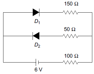
The circuit shown below contains two ideal diodes, each with a forward resistance of  If the battery voltage is
  the current through the
  resistance (in amperes) is:
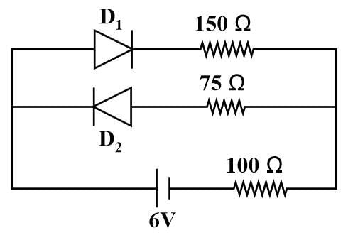
 If the battery voltage is
  the current through the
  resistance (in amperes) is:
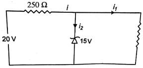
A Zener diode, having breakdown voltage equal to  is used in a voltage regulator circuit shown in the figure. The current through the diode is
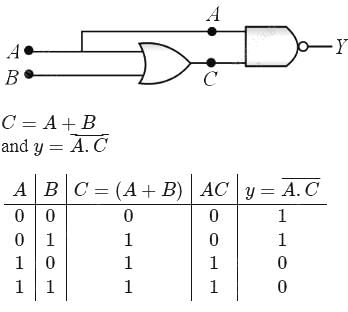
What is the Boolean expression for the gate circuit shown in Fig.

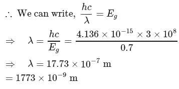
What is the maximum wavelength of electromagnetic radiation that create a electron-hole pair in material with band gap 0.7eV ? Planck's constant = 4.136 × 10¹⁵eV−s, velocity of light = 3 × 10⁸ m/s.
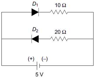
 and
and  are connected to a battery as shown in Fig. The current supplied by the battery is
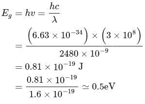
The electrical conductivity of a semiconductor increases when electromagnetic radiation of wavelength shorter than  is incident on it. The band gap energy (in
  ) for the semiconductor is
 . A minimum current of
  is required for the diode to be above the knee point. The maximum value of
  so that the voltage across the diode is above the knee point is (assume that, above the knee point, the voltage across the diode is independent of the current).
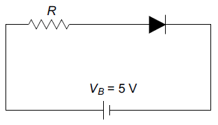
 when forward biased and
  when reverse biased. The current in the arrangement shown in Fig. will be
 th of the total current is carried by electrons and the remaining
  th by the holes. If at this temperature, the drift speed of electrons is
  times that of holes, the ratio of the number densities of electrons and holes is
 is incident on it. The bandgap (in
  ) for the semiconductor is
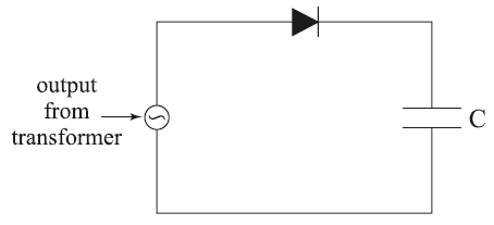
 is connected across the primary of a step-down transformer of turns ratio
  . The output of the transformer is rectified as connected in the half-wave rectifier circuit as shown in Fig. If
  , the final charge on the capacitor plates is
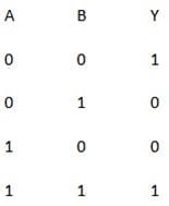
The truth tables of two logic gates P and Q are as follows.
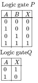
When the output of gate is connected to the input of gate , we get a new gate called
The circuit shown in Fig. contains two diodes  and
and  each with a forward resistance of 50 ohms and with infinite backward resistance. If the battery voltage is
  , the current through the
  resistance (in amperes) is
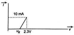
The resistance of a germanium junction diode, whose V − I characteristics is shown in the figure, will be (vk = 0.3 V).








 type is at low potential and
  type is at the higher potential a diode is in forward bias.
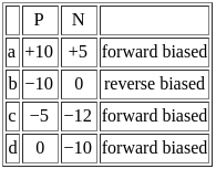
 is forward biased. Therefore, effective resistance is
  . Hence the current is
 must be
 . Hence maximum value of
  is
is
 . The current is
 Given
Given


 )
) 


 ). Hence the final charge on capacitor plates is


