Test: Digital Electronics- 2 - Electrical Engineering (EE) MCQ
20 Questions MCQ Test - Test: Digital Electronics- 2

An R — 2R ladder type DAC is shown in Figure if a switch status is '0', then 0 volt is applied and If a switch status is '1' then 5 volt is applied to the corresponding terminal of DAC.
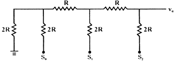
What is value of output voltage V0 for switch status so = 0, s1= 1, s2 = 1.
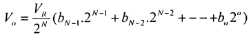
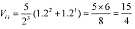
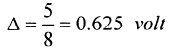
An R — 2R ladder type DAC is shown in Figure if a switch status is '0', then 0 volt is applied and If a switch status is '1' then 5 volt is applied to the corresponding terminal of DAC.
Q. What is the step size of DAC.

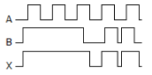
For the given circuit shown in figure signal generated at the output of AND gat is Y. there clock has signal frequency of 4 kHz, with duty cycle 50%
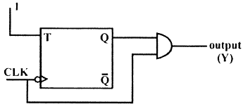
Q. What is the value of frequency of output Y
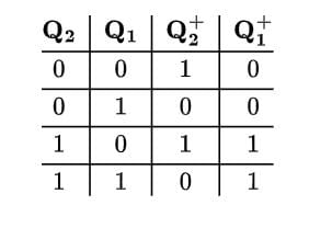
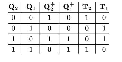
Consider the partial implementation of a 2 — bit counter using T flip-flops following the sequence 0 — 2 — 3 — 1 — 0, as shown below.
To complete the circuit, the input X should be
 Q2
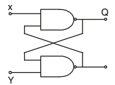
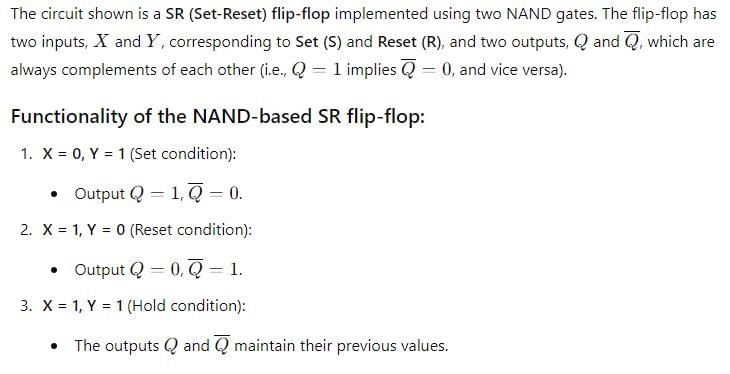
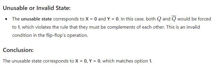
Q2For a Flip-flop formed from 2 NAND gates as shown in figure, the unusable state corresponds to
The 4 variable function f is given in terms of min term as f(A, B, C, D) = E(2,3,8,10,11,12,14,15)
Q. If by use of K-Map function is minimized in sum of product forms then SOP is
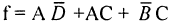
The 4 variable function f is given in terms of min term as f(A, B, C, D) = E(2,3,8,10,11,12,14,15)
Q. Above Minimised SOP, can be implemented by how many minm no. of 2 input NAND gate.
If x, y and z are three Boolean variables, then F(x,y,z) = x + xy + y + yz + z + xz is equivalent to
How many AND gates are required for a 1-to-8 multiplexer?
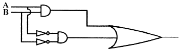
In a dual slope ADC if reference voltage is 100 mV and the first integration period is set as 50 msec.
For an input voltage of 120 mV, the second integration (de-integration) period is___ ms
In a dual slope type digital voltmeter, an unknown signal voltage is integrated our 100 cycles of clock. If the signal has a 50 Hz pick up the maximum clock frequency can be__ kHz
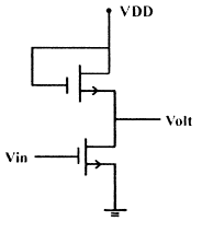
In circuit given if both Transistors have same VT what is the approximate value of highest possible output voltage vout if vh, can range from 0 to VDD, it is assumed that 0 < vT < VDD
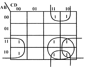
In the latch circuit shown, the NAND gates have non-zero, but unequal propagation delays. The present input condition is P = Q = 0. If the input condition is changed simultaneously to P = Q = 1, the outputs X and Y are:
In the I.C. logic gate shown in figure.
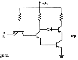
If threshold voltage VBE is o.75 volt and VCE (sat) = 0.2 V, calculate. Value of output voltage
Q. If VA = VB = 4.5 volt
For a 3-variable Boolean function F(A, B, C) = Σ(1, 3, 4, 5), what is the simplified Boolean expression for F using a K-map?
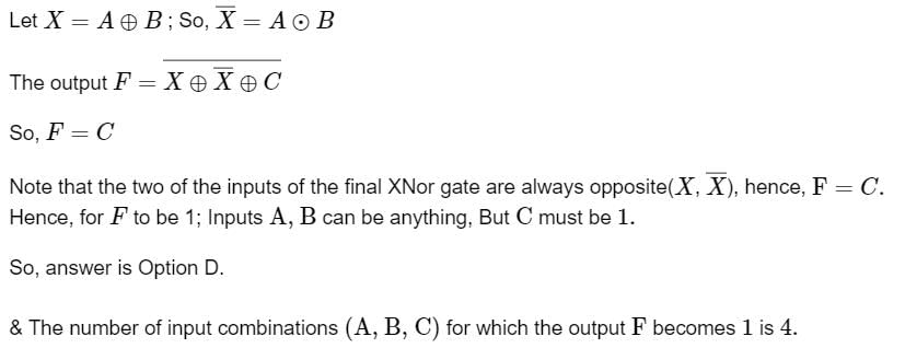
For the output F to be 1 in the logic circuit shown, the input combination should be
For a 2-bit ripple counter made using JK flip-flops, if the clock frequency is 10 kHz, what is the output frequency of the second flip-flop?
The minimum number of 2-input NAND gates required to implement a 2-input XOR gate is


Important Questions for Digital Electronics- 2
Digital Electronics- 2 MCQs with Answers
Online Tests for Digital Electronics- 2
|
© EduRev
|
Education Revolution
|


|


