Electronics and Communication Engineering (ECE) Exam  >  Electronics and Communication Engineering (ECE) Tests  >  GATE ECE (Electronics) Mock Test Series 2025  >  Test: Electronic Devices - 2 - Electronics and Communication Engineering (ECE) MCQ

Test: Electronic Devices - 2 - Electronics and Communication Engineering (ECE) MCQ


Test Description

10 Questions MCQ Test GATE ECE (Electronics) Mock Test Series 2025 - Test: Electronic Devices - 2

Test: Electronic Devices - 2 for Electronics and Communication Engineering (ECE) 2025 is part of GATE ECE (Electronics) Mock Test Series 2025 preparation. The Test: Electronic Devices - 2 questions and answers have been prepared according to the Electronics and Communication Engineering (ECE) exam syllabus.The Test: Electronic Devices - 2 MCQs are made for Electronics and Communication Engineering (ECE) 2025 Exam. Find important definitions, questions, notes, meanings, examples, exercises, MCQs and online tests for Test: Electronic Devices - 2 below.
Solutions of Test: Electronic Devices - 2 questions in English are available as part of our GATE ECE (Electronics) Mock Test Series 2025 for Electronics and Communication Engineering (ECE) & Test: Electronic Devices - 2 solutions in Hindi for GATE ECE (Electronics) Mock Test Series 2025 course. Download more important topics, notes, lectures and mock test series for Electronics and Communication Engineering (ECE) Exam by signing up for free. Attempt Test: Electronic Devices - 2 | 10 questions in 30 minutes | Mock test for Electronics and Communication Engineering (ECE) preparation | Free important questions MCQ to study GATE ECE (Electronics) Mock Test Series 2025 for Electronics and Communication Engineering (ECE) Exam | Download free PDF with solutions
Test: Electronic Devices - 2 - Question 1

Which of the following quantities cannot be measured/determined using Hall Effect?

Detailed Solution for Test: Electronic Devices - 2 - Question 1

If a semiconductor carrying current is placed in a transverse magnetic field B, an electric field E is induced in the direction perpendicular to both I and B. This phenomenon is known as the Hall Effect, it can be used to determine whether semi-conductor is n-or p-type and to find the carrier concentration and mobility.

Diffusion constant is found from electron mobility using Einstein relationship.

*Answer can only contain numeric values
Test: Electronic Devices - 2 - Question 2

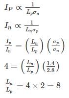
The ratio of hole diffusion current to the electron diffusion current in an infinite p-n junction is 4. If conductivity on p-side is 1.4 S/cm and on n-side is 2.8 S/cm, then the ratio of diffusion length Ln and Lp (ie Ln/Lp) is _______.


Detailed Solution for Test: Electronic Devices - 2 - Question 2

For diffusion current

Test: Electronic Devices - 2 - Question 3

Under high electric fields, in a semiconductor with increasing electric field,

Detailed Solution for Test: Electronic Devices - 2 - Question 3

we known that

V = μE

μ = constant when E < 103 V/cm
 when 103 < E < 104 V/cm
 

 when E > 104 V/cm

∴ When E Increase mobility decrease.

*Answer can only contain numeric values
Test: Electronic Devices - 2 - Question 4

The energy band structure of n-type semiconductor is as shown below
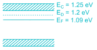
The probability that the donor energy state is empty is (up to 3 significant digits)


Detailed Solution for Test: Electronic Devices - 2 - Question 4


According to Fermi function,

Probability it is empty is 1 – F(ED) = 1 – 0.014 = 0.986

Test: Electronic Devices - 2 - Question 5

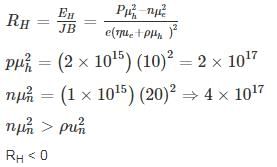
In a hypothetical semiconductor hole concentration is 2 × 10¹⁵/cm3 and electron concentration is 1 × 10¹⁵/cm3. The mobility of holes is  and mobility of electrons is  

If the specimen is subjected to hall measurement. Then the measured hall coefficient (RH) is

Detailed Solution for Test: Electronic Devices - 2 - Question 5

For a semiconductor with significant concentration of both type of carriers

*Answer can only contain numeric values
Test: Electronic Devices - 2 - Question 6

In a germanium semiconductor at 127°C has a hole concentration gradient between two points 1.5 × 10²²/m3. If the hole mobility in germanium is 800 cm2/v-s, then the diffusion current density is ______ A/m2.


Detailed Solution for Test: Electronic Devices - 2 - Question 6

Given,

T = 127°C = 400°K

μP = 800 cm2/v-s

DP = μVT

VT = kT/2 = 
⇒ DP = 800 × 0.0345 cm2/s = 27.6 cm2/s

= -1.5 × 1022 × 10-8 × 1.6 × 10-19 × 27.6 A/cm2

= -6.624 A/m2

Test: Electronic Devices - 2 - Question 7

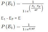
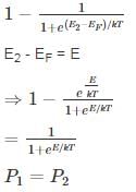
2 Consider two energy levels: E1, E eV above the Fermi level and E2, EeV below the Fermi level. P1 and P2 are respectively the probabilities of E1 being occupied by an electron and E2 being empty. Then

Detailed Solution for Test: Electronic Devices - 2 - Question 7

Case 1:

E1 ⇒ EeV above the fermi level probability of E1 being occupied by on electron = P(E1)


Case II:

E2 → EeV below the fermi level probability of E2 being occupied

Probability of E2 being empty:

*Answer can only contain numeric values
Test: Electronic Devices - 2 - Question 8

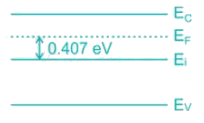
A silicon sample is dope with unknown concentration of Arsenic, such that the fermi level (EF) is 0.407 eV relative to intrinsic level (Ei). The conductivity of the silicon sample after doping is______(Ω – cm)-1.

The mobility of electrons μn = 3800 cm2/v-s and holes μp = 1800 cm2/v-s. Take kT = 0.0259 eV at 300°K and intrinsic concentration ni = 1.5 × 1010 cm-3


Detailed Solution for Test: Electronic Devices - 2 - Question 8

Given, Si sample is doped with As (donor impurity) and the band structure is


Let nd be doping concentration, hence the electron concentration also is nd.

The extrinsic electron concentration is related to intrinsic concentration by


∴ Conductivity σ = μndq

= 3800 × 1 × 1017 × 1.6 × 10-19

= 60.8 (Ω - cm)-1

Test: Electronic Devices - 2 - Question 9

The effective density of states in conduction and valence band NC and Nv at 300K is 4.7x1017 cm−3 and 7x1018cm−3 respectively. The bandgap of the mentioned semiconductor is 1.42eV at 300K. The intrinsic carrier concentration is:

Use Boltzmann constant k = 8.62 x 10⁻⁵ eV/K

Detailed Solution for Test: Electronic Devices - 2 - Question 9

Given
Nc = 4.7 x 1017 cm−3
Nv = 7 x 1018 cm−3

Eg = 1.42 eV
Now,

*Answer can only contain numeric values
Test: Electronic Devices - 2 - Question 10

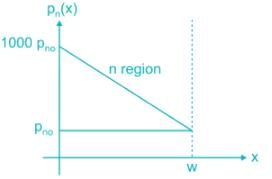
Holes are being steadily injected into a region of n-type silicon. In the steady state, the excess hole concentration profile is shown. [The term excess means over and above concentrations pno]

If  Dp = 12 cm2/sec ND = 1016/cm3, ni = 1.5 × 10¹⁰/cm3 and w = 5 μm.

The current density that will flow in x-direction is _____ nA/cm2.

Detailed Solution for Test: Electronic Devices - 2 - Question 10

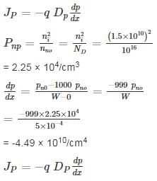
The diffusion current density is given by

= -4.49 × 10¹⁰/cm4


= -1.6 × 10-19 × 12 × (-4.49 × 10¹⁰)

= 8.64 × 10⁻⁸ A/cm2

= 86.4 × 10⁻⁹ nA/cm2

25 docs|263 tests
Information about Test: Electronic Devices - 2 Page
In this test you can find the Exam questions for Test: Electronic Devices - 2 solved & explained in the simplest way possible. Besides giving Questions and answers for Test: Electronic Devices - 2, EduRev gives you an ample number of Online tests for practice
Download as PDF