Test: BJT Characteristics & Biasing- 2 - Electrical Engineering (EE) MCQ
15 Questions MCQ Test - Test: BJT Characteristics & Biasing- 2

The CE configuration amplifier circuits are preferred over CB configuration amplifier circuits because they have
A device whose characteristics are very close to that of an ideal current source is

The input resistance of a common-collector configuration will be of the order of
The common collector amplifier is also Known as
Consider the statements associated with various types of transistor configuration of a BJT:
1. In cut-off region, emitter and collector junctions are both reverse biased.
2. In saturation region, emitter junction is forward biased while collector junction can be either forward biased or reverse biased.
3. In active region, the collector junction is biased in the reverse biased and the emitter junction in the forward biased.
4. The phase shift introduced to the input in CC and CE configurations are each zero degree.
Q. Which of the above statements are correct ?
In an n-p-n transistor biased in the active region:
Assertion (A): An emitter follower is widely used in electronic instruments.
Reason (R): The voltage gain of emitter follower is very high.
Assertion (A): Common base amplifier has very low input resistance.
Reason (R): Low emitter ac resistance r'e shunts all other resistances.
Consider the following statements:
1. In a p-n-p transistor with normal bias, the collector junction is of low resistance.
2. p-n-p and n-p-n transistors can be interchanged with each other.
3. The circuit arrangement of a transistor used as a buffer is CC (Common Collector).
4. In a CE connected transistor, VCE will be equal to VCC when base current is zero.
5. In a transistor, emitter junction breakdown is due to “Zener effect” while collector junction breakdown is due to “Avalanche effect”.
Q. Which of the statements given above are not correct ?
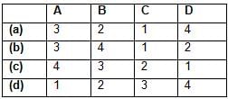
Match List-I with List-II and select the correct answer using the codes given below the lists:
List-I
A. Common emitter Configuration
B. Common collector Configuration
C. Base width modulation
D. Common base Configuration
List-II
1. Early Effect
2. Highest input resistance
3. Inverting amplifier
4. Lowest power gain
Codes:
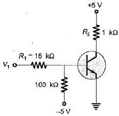
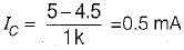
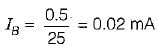
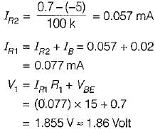
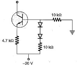
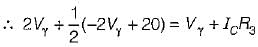
For the transistor shown in the figure below, β = 25. The range of V1 such that, 1.0 < VCE < 4.5 V is
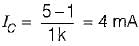
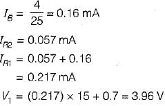
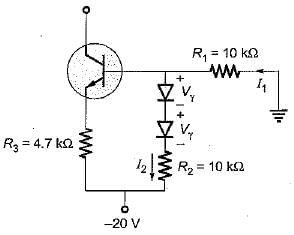
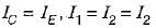
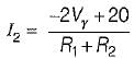
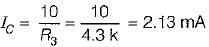
In the bipolar source of figure the diode voltage and transistor VBE voltages are equal. If base current is neglected then collector current is
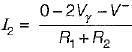
 ..(i)
..(i)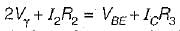 ..(ii)
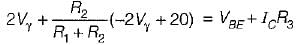


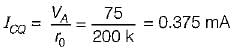
The Early voltage of a BJT is VA = 75 volt. The minimum required collector current, such that the output resistance is atleast r0 = 200 KΩ is

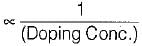
The thinnest region in a BJT is_____and the most doped region is________.
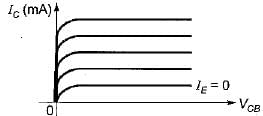
In an n-p-n transistor biased in the active region, as the magnitude of the collector-base voltage is increased,
Important Questions for BJT Characteristics & Biasing- 2
BJT Characteristics & Biasing- 2 MCQs with Answers
Online Tests for BJT Characteristics & Biasing- 2
|
© EduRev
|
Education Revolution
|


|


within 7 days!