Test: Operational Amplifiers - Electronics and Communication Engineering (ECE) MCQ
20 Questions MCQ Test GATE ECE (Electronics) Mock Test Series 2025 - Test: Operational Amplifiers
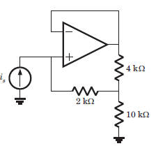
For the circuit shown in fig. the input resistance is

In the circuit of fig. the op-amp slew rate is SR = 0.5 V/μs. If the amplitude of input signal is 0.02 V, then the maximum frequency that may be used is

In the circuit of fig. the input offset voltage and input offset current are Vio = 4 mV and Iio = 150 nA. The total output offset voltage is

If ‘V’ is the voltage phasor and ‘I’ is the current phasor, then VI represents
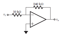
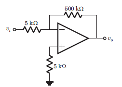
Consider the circuit shown below
Que: If vi = -2 V, then output vo is
The circuit shown in fig. is at steady state before the switch opens at t = 0. The vc(t) for t > 0 is
In the circuit of fig. the CMRR of the op-amp is 60 dB. The magnitude of the vo is
The analog multiplier X of fig. has the characteristics vp = v1v2 The output of this circuit is
If the input to the ideal comparator shown in fig. is a sinusoidal signal of 8 V (peak to peak) without any DC component, then the output of the comparator has a duty cycle of
In the op-amp circuit given in fig. the load current iL is
In the circuit of fig. output voltage is |vo| =1 V for a certain set of ω, R, an C. The |vo| will be 2 V if
The phase shift oscillator of fig. operate at f = 80 kHz. The value of resistance RF is
The value of C required for sinusoidal oscillation of frequency 1 kHz in the circuit of fig. is
In the circuit shown in fig. the op-amp is ideal. If βF = 60, then the total current supplied by the 15 V source is
In the circuit in fig. both transistor Q1 and Q2 are identical. The output voltage at T = 300 K is
In the op-amp series regulator circuit of fig. Vz = 62. V, VBE = 0.7 V and β = 60. The output voltage vo is
|
25 docs|263 tests
|


