Test: Transistor Biasing & Thermal Stabilization- 2 - Electrical Engineering (EE) MCQ
15 Questions MCQ Test GATE Electrical Engineering (EE) Mock Test Series 2026 - Test: Transistor Biasing & Thermal Stabilization- 2

Assertion (A): Current mirrors are widely used in analog integrated circuits for DC biasing.
Reason (R): Current mirrors provide highly stable DC bias points without the need of a lot of biasing resistors.
Reason (R): Current mirrors provide highly stable DC bias points without the need of a lot of biasing resistors.
Consider the following statements:
1. Self-blas is superior to the fixed bias from the consideration of stability of operating point in the CE amplifier.
2. Bias stabilization is used to prevent thermal runaway.
3. Improper biasing of a transistor results in the distortion of the output signal.
4. A transistor is said to be in quiescent stage when no signal is applied to the input.
Q. Which of the statements given above are correct?
1. Self-blas is superior to the fixed bias from the consideration of stability of operating point in the CE amplifier.
2. Bias stabilization is used to prevent thermal runaway.
3. Improper biasing of a transistor results in the distortion of the output signal.
4. A transistor is said to be in quiescent stage when no signal is applied to the input.

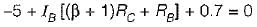
For the circuit shown below, what is the value of RC needed if VC = 2 V ?
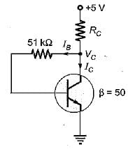
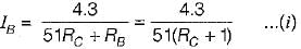
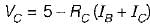
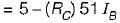
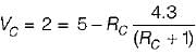 (Using equation (i))
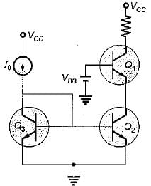
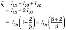
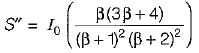
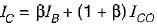
Assuming the current source to be ideal, all transistors to be identical, and IC = βIB the stability factor  for the current mirror circuit shown below would be
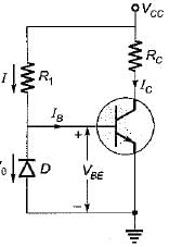
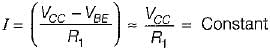
A reverse biased diode placed in parallel with the base-emitter junction makes the circuit insensitive to variations in______with changes in temperature.
The static (DC) and dynamic (AC) load lines in a transistor amplifier are different when
Thermal runaway is not possible in FET because as the temperature of FET increases,
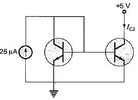
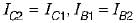
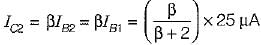
The two transistors in figure are identical. If β = 25, the current IC2 is

The input resistance of a common emitter stage can be increased by
1. unbypassing emitter resistance
2. bootstrapping
3. biasing it at low quiescent current
4. using compounded BJTs
Q. The correct sequence in descending order of the effectiveness of these methods is
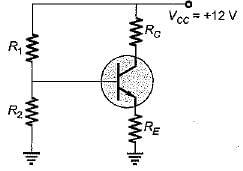
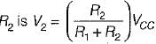
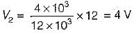
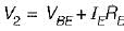
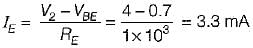
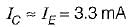
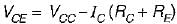
For the transistor amplifier shown in figure below, VCC = 12 V, R1, = 8 kΩ, R2 = 4 kΩ, RC = 1 kΩ, RE = 1 kΩ.
Assuming VBE = 0.7 V, the operating point Q be given as
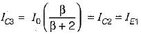
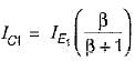
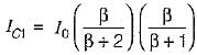
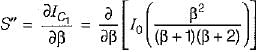
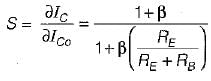
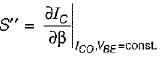
In a self bias circuit using BJT, if the stability factor is represented as  then the rate of change of IC w.r.t. β, keeping ICO and VBE constant will be given by (IC= collector current of the transistor)

The forward current gain (α) of a bipolar transistor can be increased by
1. reducing the recombination lifetime in the emitter
2. increasing the emitter doping density.
3. increasing the base doping density.
4. reducing the base width.
Select the correct code from the given options,
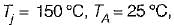
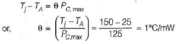
What is the value of thermal resistance for the 2N338 transistor for which the manufacturer specifies PC,max = 125 mW at 25°C free-air temperature and maximum junction temperature of 150°C?
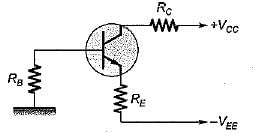
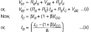
The stability factor (S1) for the circuit shown below is given by
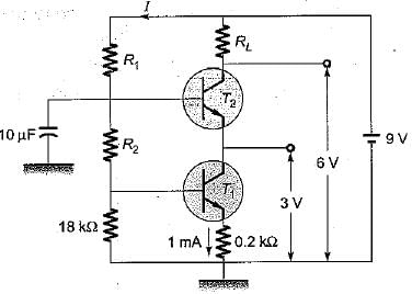
For the cascade amplifier shown below, the quiescent current through transistors is 1.mA and the collector voltage VC2 = 6 V and VC1 = 3 V. Assuming VBE = 0.7 V and very high Value of β, the values of R1 and R2 will be respectively
|
26 docs|257 tests
|
|
26 docs|257 tests
|
Important Questions for Transistor Biasing & Thermal Stabilization- 2
Transistor Biasing & Thermal Stabilization- 2 MCQs with Answers
Online Tests for Transistor Biasing & Thermal Stabilization- 2 GATE Electrical Engineering (EE) Mock Test Series 2026
|
© EduRev
|
Education Revolution
|


|


within 7 days!