Electrical Engineering (EE) Exam  >  Electrical Engineering (EE) Tests  >  Topicwise Question Bank for Electrical Engineering  >  Test: Digital Electronics- 2 - Electrical Engineering (EE) MCQ

Test: Digital Electronics- 2 - Electrical Engineering (EE) MCQ


Test Description

19 Questions MCQ Test Topicwise Question Bank for Electrical Engineering - Test: Digital Electronics- 2

Test: Digital Electronics- 2 for Electrical Engineering (EE) 2024 is part of Topicwise Question Bank for Electrical Engineering preparation. The Test: Digital Electronics- 2 questions and answers have been prepared according to the Electrical Engineering (EE) exam syllabus.The Test: Digital Electronics- 2 MCQs are made for Electrical Engineering (EE) 2024 Exam. Find important definitions, questions, notes, meanings, examples, exercises, MCQs and online tests for Test: Digital Electronics- 2 below.
Solutions of Test: Digital Electronics- 2 questions in English are available as part of our Topicwise Question Bank for Electrical Engineering for Electrical Engineering (EE) & Test: Digital Electronics- 2 solutions in Hindi for Topicwise Question Bank for Electrical Engineering course. Download more important topics, notes, lectures and mock test series for Electrical Engineering (EE) Exam by signing up for free. Attempt Test: Digital Electronics- 2 | 19 questions in 60 minutes | Mock test for Electrical Engineering (EE) preparation | Free important questions MCQ to study Topicwise Question Bank for Electrical Engineering for Electrical Engineering (EE) Exam | Download free PDF with solutions
*Answer can only contain numeric values
Test: Digital Electronics- 2 - Question 1

In the circuit sho

Qo = Q1 = 0 Then the values of QO and QI after 335th clock pulse are _____________


Detailed Solution for Test: Digital Electronics- 2 - Question 1

To solve this problem, we need to understand the circuit shown in the image. The circuit appears to be a series of flip-flops connected in such a way that they create a ripple counter or a type of sequential circuit. Here's how we can approach it:

Test: Digital Electronics- 2 - Question 2

An R — 2R ladder type DAC is shown in Figure if a switch status is '0', then 0 volt is applied and If a switch status is '1' then 5 volt is applied to the corresponding terminal of DAC.
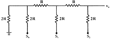
What is value of output voltage V0 for switch status so = 0, s1= 1, s2 = 1.


Detailed Solution for Test: Digital Electronics- 2 - Question 2

1 Crore+ students have signed up on EduRev. Have you? Download the App
Test: Digital Electronics- 2 - Question 3

An R — 2R ladder type DAC is shown in Figure if a switch status is '0', then 0 volt is applied and If a switch status is '1' then 5 volt is applied to the corresponding terminal of DAC.

Q. What is the step size of DAC.

Detailed Solution for Test: Digital Electronics- 2 - Question 3

Step size

Test: Digital Electronics- 2 - Question 4

For the given circuit shown in figure signal generated at the output of AND gat is Y. there clock has signal frequency of 4 kHz, with duty cycle 50%
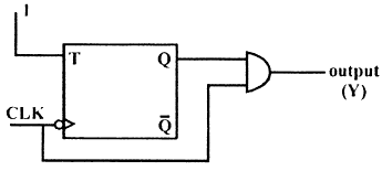
Q. What is the value of frequency of output Y

Detailed Solution for Test: Digital Electronics- 2 - Question 4

A FF is simply MOD-2 counter.

Test: Digital Electronics- 2 - Question 5

The following waveform pattern is for a(n) ________.

Test: Digital Electronics- 2 - Question 6

Consider the partial implementation of a 2 — bit counter using T flip-flops following the sequence 0 — 2 — 3 — 1 — 0, as shown below.


To complete the circuit, the input X should be 

Detailed Solution for Test: Digital Electronics- 2 - Question 6

Sequence is  0 — 2 — 3 — 1 — 0 
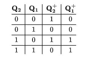
From the given sequence, we have state table as

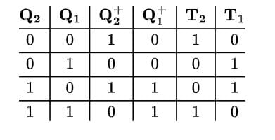
Now we have present state and next state, use excitation table of T flip-flop


Correct option: a) Q Q2

Test: Digital Electronics- 2 - Question 7

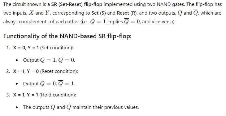
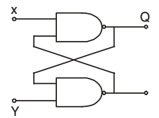
 For a Flip-flop formed from 2 NAND gates as shown in figure, the unusable state corresponds to
Detailed Solution for Test: Digital Electronics- 2 - Question 7


Test: Digital Electronics- 2 - Question 8

In the figure as long as XI = 1 and X2 = 1 the output Q remains at

Detailed Solution for Test: Digital Electronics- 2 - Question 8

As long as X1 = 1 and X2 = 1
Since the output is feedback to input NAND gate. It means output is toggle between 0 → 1 → 0 → 1…… makes the output Q unstable.

*Answer can only contain numeric values
Test: Digital Electronics- 2 - Question 9

The Minimum no. of 2 inputs NAND gate required to implement Boolean function f(A, B, C, D) =

ABCD are_______


Detailed Solution for Test: Digital Electronics- 2 - Question 9

Correct Answer :- 6

Explanation :  

Test: Digital Electronics- 2 - Question 10

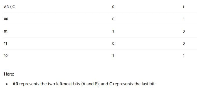
The 4 variable function f is given in terms of min term as f(A, B, C, D) = E(2,3,8,10,11,12,14,15)

Q. If by use of K-Map function is minimized in sum of product forms then SOP is

Detailed Solution for Test: Digital Electronics- 2 - Question 10

Test: Digital Electronics- 2 - Question 11

The 4 variable function f is given in terms of min term as f(A, B, C, D) = E(2,3,8,10,11,12,14,15)

Q. Above Minimised SOP, can be implemented by how many minm no. of 2 input NAND gate.

Detailed Solution for Test: Digital Electronics- 2 - Question 11

*Answer can only contain numeric values
Test: Digital Electronics- 2 - Question 12

Consider the following data in respect of a certain digital gate

loH = 0.2 mA I1H= 40μ.A, 10L = 16 mA, liL = 1.6 mA symbols have their meaning. Fan out will be    


Detailed Solution for Test: Digital Electronics- 2 - Question 12

F.0 = = 5

Smalls of both will be Fan out

F.I = =10

Test: Digital Electronics- 2 - Question 13

If x, y and z are three Boolean variables, then F(x,y,z) = x + xy + y + yz + z + xz is equivalent to

Test: Digital Electronics- 2 - Question 14

How many AND gates are required for a 1-to-8 multiplexer?

Detailed Solution for Test: Digital Electronics- 2 - Question 14

The number of AND gates required will be equal to the number of outputs in a demultiplexer.

Test: Digital Electronics- 2 - Question 15

The logic circuit shown in figure is :

*Answer can only contain numeric values
Test: Digital Electronics- 2 - Question 16

In a dual slope ADC if reference voltage is 100 mV and the first integration period is set as 50 msec.

For an input voltage of 120 mV, the second integration (de-integration) period is___ ms


Detailed Solution for Test: Digital Electronics- 2 - Question 16

t = 60 m sec

*Answer can only contain numeric values
Test: Digital Electronics- 2 - Question 17

In a dual slope type digital voltmeter, an unknown signal voltage is integrated our 100 cycles of clock. If the signal has a 50 Hz pick up the maximum clock frequency can be__ kHz


Detailed Solution for Test: Digital Electronics- 2 - Question 17

50 x 100

Test: Digital Electronics- 2 - Question 18

In circuit given if both Transistors have same VT what is the approximate value of highest possible output voltage vout if vh, can range from 0 to VDD, it is assumed that 0 < vT < VDD

Test: Digital Electronics- 2 - Question 19

In the I.C. logic gate shown in figure.

If threshold voltage VBE is o.75 volt and VCE (sat) = 0.2 V, calculate. Value of output voltage

Q. If VA = VB = 4.5 volt

Detailed Solution for Test: Digital Electronics- 2 - Question 19

It is A NAND gate and if VA= VB = 4.5
Then o/p will be logic zero, as both are logic high

SO V0 = VCE, sat = 0•2v

212 tests
Information about Test: Digital Electronics- 2 Page
In this test you can find the Exam questions for Test: Digital Electronics- 2 solved & explained in the simplest way possible. Besides giving Questions and answers for Test: Digital Electronics- 2, EduRev gives you an ample number of Online tests for practice

Top Courses for Electrical Engineering (EE)

Download as PDF

Top Courses for Electrical Engineering (EE)