Electrical Engineering (EE) Exam  >  Electrical Engineering (EE) Tests  >  GATE Electrical Engineering (EE) Mock Test Series 2025  >  Test: Power Semiconductor Diode & Transistors - Electrical Engineering (EE) MCQ

Test: Power Semiconductor Diode & Transistors - Electrical Engineering (EE) MCQ


Test Description

10 Questions MCQ Test GATE Electrical Engineering (EE) Mock Test Series 2025 - Test: Power Semiconductor Diode & Transistors

Test: Power Semiconductor Diode & Transistors for Electrical Engineering (EE) 2025 is part of GATE Electrical Engineering (EE) Mock Test Series 2025 preparation. The Test: Power Semiconductor Diode & Transistors questions and answers have been prepared according to the Electrical Engineering (EE) exam syllabus.The Test: Power Semiconductor Diode & Transistors MCQs are made for Electrical Engineering (EE) 2025 Exam. Find important definitions, questions, notes, meanings, examples, exercises, MCQs and online tests for Test: Power Semiconductor Diode & Transistors below.
Solutions of Test: Power Semiconductor Diode & Transistors questions in English are available as part of our GATE Electrical Engineering (EE) Mock Test Series 2025 for Electrical Engineering (EE) & Test: Power Semiconductor Diode & Transistors solutions in Hindi for GATE Electrical Engineering (EE) Mock Test Series 2025 course. Download more important topics, notes, lectures and mock test series for Electrical Engineering (EE) Exam by signing up for free. Attempt Test: Power Semiconductor Diode & Transistors | 10 questions in 30 minutes | Mock test for Electrical Engineering (EE) preparation | Free important questions MCQ to study GATE Electrical Engineering (EE) Mock Test Series 2025 for Electrical Engineering (EE) Exam | Download free PDF with solutions
Test: Power Semiconductor Diode & Transistors - Question 1

In a Schottky diode junction is formed between

Detailed Solution for Test: Power Semiconductor Diode & Transistors - Question 1

In a Schottky diode junction is formed between metal and semiconductor

Test: Power Semiconductor Diode & Transistors - Question 2

Assertion (A) : A Schottky diode has very high reverse voltage rating as compared to alloyed and diffused diodes.
Reason (R) : In a Schottky diode the metallic layer is surrounded by a ring of insulating material such as SiO2.

Detailed Solution for Test: Power Semiconductor Diode & Transistors - Question 2

A Schottky diode has very low reverse voltage rating as compared to alloyed and diffused diodes. Maximum voltage rating is about 100 V. Thus, assertion is a false statement.
In a schottky diode, a thin epitaxial layer is grown on n-type base (substrate). On the epitaxial layer metal (gold, chromium or platinum) is deposited to form a thin layer. This metallic layer is surrounded by a ring of insulating material such as SiO2. Thus reason is a true statement.

Test: Power Semiconductor Diode & Transistors - Question 3

Consider the following statements:
1. By increasing the rate of recombination and removal of minority carrier, reverse recovery period can be reduced.
2. In fast recovery diode, rate of recombination is decreased.
3. MOSFET and transistors are used in high power applications.
4. IGBT is having all the good properties of a transistors and MOSFET.

Which of the statements given above are correct?

Detailed Solution for Test: Power Semiconductor Diode & Transistors - Question 3
  • In fast recovery diode, reverse recovery time is reduced by addition of gold or platinum due to which rate of recombination is increased. Hence, statements-2 is not correct.
  • MOSFET and transistor are used in low and medium power applications. Thus, statements-3 is not correct.
Test: Power Semiconductor Diode & Transistors - Question 4

A power transistor
1. cannot be easily paralleled.
2. is susceptible to secondary breakdown.
3. has low transconductance than MOSFET.
4. has negative temperature coefficient on collector current.
5. has low switching speed than MOSFET

Which of the above characteristics are possessed by a power transistor?

Detailed Solution for Test: Power Semiconductor Diode & Transistors - Question 4

A power transistor
1. can not be easily paralleled because of Vbe matching problems and local current concentration.
2. is susceptible to secondary breakdown.
3. has high transconductance.
4. has positive temperature coefficient on collector current since Ic in creases with temperature.
5. has low switching speed than MOSFET.

Test: Power Semiconductor Diode & Transistors - Question 5

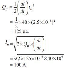
The rate of fall of diode current for a diode is 40 A/ms and reverse recovery time is 2.5 ms. The Peak reverse current (assuming the softness factor as 0.5) is given by

Detailed Solution for Test: Power Semiconductor Diode & Transistors - Question 5

Test: Power Semiconductor Diode & Transistors - Question 6

Which of the following are not a unidirectional current devices?
1. BJT
2. TRIAC 
3. SCR
4. GTO
5. IGBT

Detailed Solution for Test: Power Semiconductor Diode & Transistors - Question 6

TRIAC is a bidirectional device whereas BJT, GTO, SCR  and IGBT are unidirectional devices.

Test: Power Semiconductor Diode & Transistors - Question 7

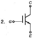
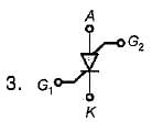
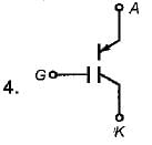
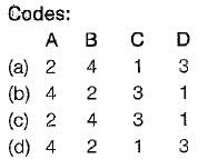
Match List-I (Power devices) with List-Il (Symbols) and select the correct answer using the codes given below the lists:
List-I 
A. IGBT
B. MCT
C. Programmable Unijunction Transistor (PUT)
D. Silicon Controlled Switch (SCS)

List-II


Test: Power Semiconductor Diode & Transistors - Question 8

Assertion (A): With increased reverse bias, the reverse blocking safe operating area increases in size.
Reason (R): The reverse blocking safe operating area is a plot of collector current versus collector-emitter voltage.

Detailed Solution for Test: Power Semiconductor Diode & Transistors - Question 8

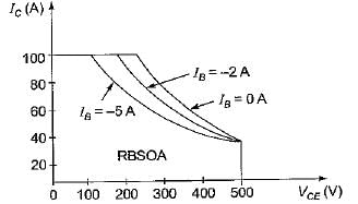
The reverse blocking safe operating area (RBSOA) for a power transistor is shown below.

It is clear from above curve that with increased reverse bias, the RBSOA decreases in size.

Test: Power Semiconductor Diode & Transistors - Question 9

A power transistor has its switching, waveforms as shown in figure. If the average power loss in the transistor is limited to 300 W, the switching frequency at which the transistor can be operated is approximately equal to
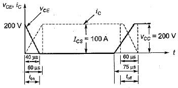
Detailed Solution for Test: Power Semiconductor Diode & Transistors - Question 9


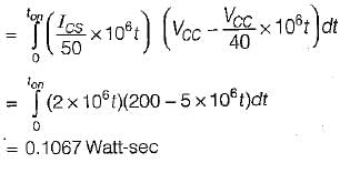
Energy loss during turn-off

= 0.1603 Watt-sec
Total energy loss in one cycle
= 0.1067 + 0.1603 
= 0.267 W-sec
Average power loss in transistor
= Switching frequency x energy loss in one cycle
∴ Allowable switching frequency

Test: Power Semiconductor Diode & Transistors - Question 10

Which one of the following suited for current controlled device

Detailed Solution for Test: Power Semiconductor Diode & Transistors - Question 10

BJTcan easily turn on and turn off using base current.

25 docs|247 tests
Information about Test: Power Semiconductor Diode & Transistors Page
In this test you can find the Exam questions for Test: Power Semiconductor Diode & Transistors solved & explained in the simplest way possible. Besides giving Questions and answers for Test: Power Semiconductor Diode & Transistors, EduRev gives you an ample number of Online tests for practice
Download as PDF