Electronics and Communication Engineering (ECE) Exam  >  Electronics and Communication Engineering (ECE) Tests  >  Analog Circuits  >  Test: BJT in Amplifier Design - Electronics and Communication Engineering (ECE) MCQ

Test: BJT in Amplifier Design - Electronics and Communication Engineering (ECE) MCQ


Test Description

10 Questions MCQ Test Analog Circuits - Test: BJT in Amplifier Design

Test: BJT in Amplifier Design for Electronics and Communication Engineering (ECE) 2024 is part of Analog Circuits preparation. The Test: BJT in Amplifier Design questions and answers have been prepared according to the Electronics and Communication Engineering (ECE) exam syllabus.The Test: BJT in Amplifier Design MCQs are made for Electronics and Communication Engineering (ECE) 2024 Exam. Find important definitions, questions, notes, meanings, examples, exercises, MCQs and online tests for Test: BJT in Amplifier Design below.
Solutions of Test: BJT in Amplifier Design questions in English are available as part of our Analog Circuits for Electronics and Communication Engineering (ECE) & Test: BJT in Amplifier Design solutions in Hindi for Analog Circuits course. Download more important topics, notes, lectures and mock test series for Electronics and Communication Engineering (ECE) Exam by signing up for free. Attempt Test: BJT in Amplifier Design | 10 questions in 10 minutes | Mock test for Electronics and Communication Engineering (ECE) preparation | Free important questions MCQ to study Analog Circuits for Electronics and Communication Engineering (ECE) Exam | Download free PDF with solutions
Test: BJT in Amplifier Design - Question 1

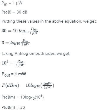
Linear amplifier with a gain of 30 dB is fed with 1.0 μW power. The output power of the amplifier

Detailed Solution for Test: BJT in Amplifier Design - Question 1

Test: BJT in Amplifier Design - Question 2

The corresponding maximum input signal permitted is

Detailed Solution for Test: BJT in Amplifier Design - Question 2

If we assume linear operation right to saturation we can use the gain Av to calculate the maximum input signal. Thus for an output swing ∆ Vo = 0.8 we have
∆ Vi = ∆ Vo / Av = -0.7 / -360 = 1.94 mV.

1 Crore+ students have signed up on EduRev. Have you? Download the App
Test: BJT in Amplifier Design - Question 3

(Q.3- Q.5) For the amplifier circuit in Fig. 6.33(a) with Vcc = +10 V, Rc = 1 kΩ and the DC collector bias current equal to Ic

Q. Find the voltage gain.

Detailed Solution for Test: BJT in Amplifier Design - Question 3

Test: BJT in Amplifier Design - Question 4

The maximum possible positive output signal swing as determined by the need to keep the transistor in the active region.

Detailed Solution for Test: BJT in Amplifier Design - Question 4

Assuming the output voltage Vo = 0.3v is the lowest Vce to stay out of saturation.
Vo = 0.3 = 10 – IcRc
= 10 – IcRc + ∆Vo
∆ Vo = -10 + 0.3 + Ic*1.

Test: BJT in Amplifier Design - Question 5

The maximum possible negative output signal swing as determined by the need to keep the transistor in the active region.

Detailed Solution for Test: BJT in Amplifier Design - Question 5

Maximum output voltage before the Transistor is cutoff.
Vce + ∆Vo = Vcc
∆Vo = Vcc – Vce
= 10 – 10 + 10 Ic
= 10 Ic.

Test: BJT in Amplifier Design - Question 6

The transistor in the circuit below is biased at a dc collector current of 0.5 mA. What is the voltage gain?

Detailed Solution for Test: BJT in Amplifier Design - Question 6

Test: BJT in Amplifier Design - Question 7

For a BJt Vt is 5 V, Rc = 1000 ohm and bias current Ic is 12 mA. The value of the voltage gain is __________

Detailed Solution for Test: BJT in Amplifier Design - Question 7

Voltage gain is (Ic X Rc ) / Vt.

Test: BJT in Amplifier Design - Question 8

(Q.8–Q.10) (Q.3- Q.5) For the BJT amplifier circuit with Vcc = +10 V, Rc = 1 kΩ and the DC collector bias current equal to 5 mA,

Q. The value of the voltage gain is _______________

Detailed Solution for Test: BJT in Amplifier Design - Question 8

The voltage is 400 X Ic where Ic is 5 mA.

Test: BJT in Amplifier Design - Question 9

The maximum possible positive output signal swing as determined by the need to keep the transistor in the active region.

Detailed Solution for Test: BJT in Amplifier Design - Question 9

The maximum voltage swing is given by -10 + 0.3 + (Ic X Rc). Putting Ic as 5 mA, we get -4.7 mV.

Test: BJT in Amplifier Design - Question 10

The maximum possible negative output signal swing as determined by the need to keep the transistor in the active region.

Detailed Solution for Test: BJT in Amplifier Design - Question 10

 It is given by -10 + 10 + (Ic X Rc). Putting Ic as 5 mA we get 5V.

3 videos|33 docs|64 tests
Information about Test: BJT in Amplifier Design Page
In this test you can find the Exam questions for Test: BJT in Amplifier Design solved & explained in the simplest way possible. Besides giving Questions and answers for Test: BJT in Amplifier Design, EduRev gives you an ample number of Online tests for practice

Top Courses for Electronics and Communication Engineering (ECE)

3 videos|33 docs|64 tests
Download as PDF

Top Courses for Electronics and Communication Engineering (ECE)