ISRO Scientist Electronics Mock Test - 2 - Electronics and Communication Engineering (ECE) MCQ
30 Questions MCQ Test - ISRO Scientist Electronics Mock Test - 2

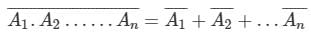
The Fourier transform X(jω) of the signal

is _______.

 2π x(-ω)
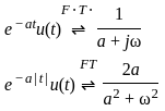

 ....(1)
 X(ω)
X(ω) j
j 
 .....(2)
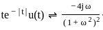
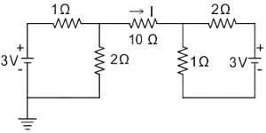
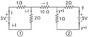
Consider the circuit shown in the figure. The current I flowing through the 10 Ω resistor is _________.

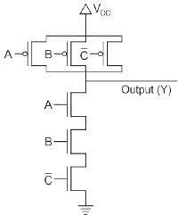
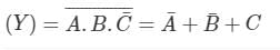
The output (Y) of the circuit shown in the figure is

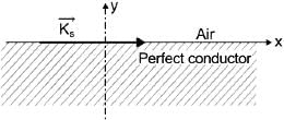
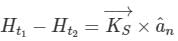
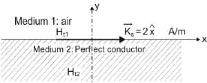
A region shown below contains a perfect conducting half-space and air. The surface current  on the surface of the perfect conductor is
  amperes per meter. The tangential
  field in the air just above the perfect conductor is


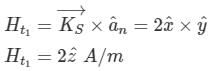
A thin P-type silicon sample is uniformly illuminated with light which generates excess carriers. The recombination rate is directly proportional to
Assuming that the Op-amp in the circuit shown is ideal, Vo is given by
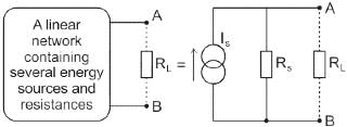
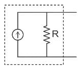
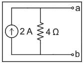
Norton’s theorem states that a complex network connected to a load can be replaced with an equivalent impedance

 ---(2)
 ---(1)
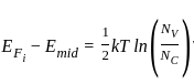
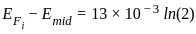
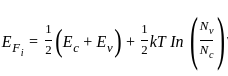
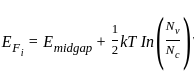
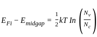
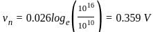
 is shifted from the mid-bandgap energy level by 9.01 meV.
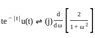
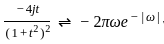
A discrete time signal,
x[n] = 2 sin(π2n), n being an integer, is
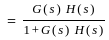
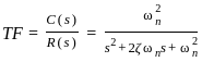
The open loop transfer function of a unity negative feedback control system is given by 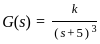


 ---(1)
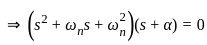
 ---(2)

For a casual LTI system the impulse response is 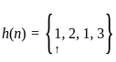 . What will be the system difference equation?

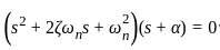
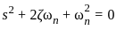
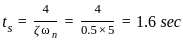
The second-order system defined by  is given a step input. The time taken for the output to settle within ± 2% is
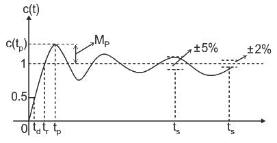
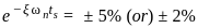
 for a 5% tolerance band.
 for 2% tolerance band
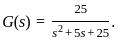


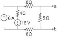
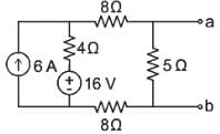
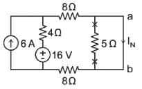
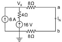
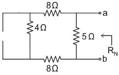
Find the Norton equivalent circuit of the circuit in Fig. at terminals a-b.
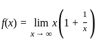
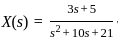
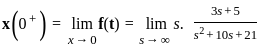
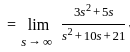
The Laplace transform of a causal signal x(t) is X(s) =  . The value of the signal x(t) at t = 1 sec is:
(Take e-3 ≈ 0.05)


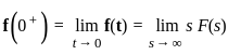
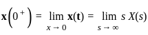
 be the Laplace Transform of a signal x(t). Then x(0+) is

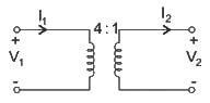
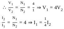
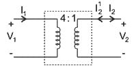
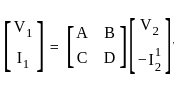
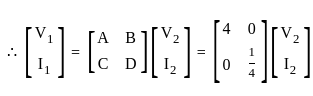
Find the ABCD parameters of an ideal transformer given below

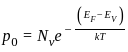
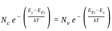
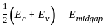
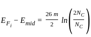
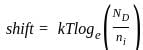
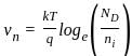
A Si n-type semiconductor is doped with donor impurity of 1016 cm-3 at room temperature if the intrinsic concentration is 1010 cm-3 then the gap between Fermi energy level and intrinsic energy level is
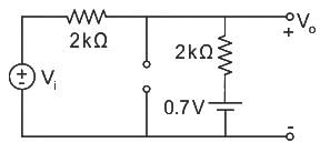
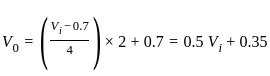
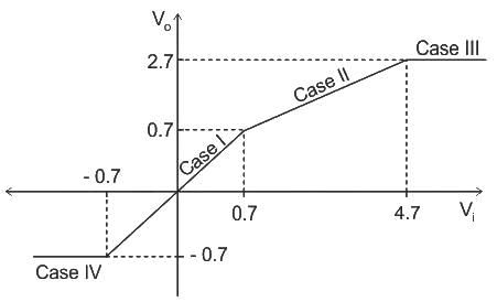
Consider a circuit given below:
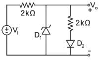
The cut in voltage of the diode is 0.7 V and the breakdown voltage of the Zener diode is 2.7 V.
The correct transfer characteristics is ________
The root of f(x) = x3 - 3x2 + 1 lies in:
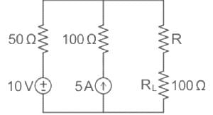
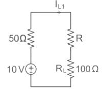
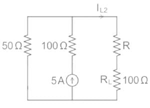
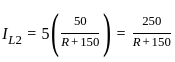
Find the value of R (in ohms) such that maximum power transfers to the load resistance RL.


The given bar diagram represents the number of persons who have taken an insurance policy on the y-axis, and the year of purchase of the insurance policy on the x-axis.
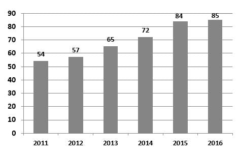
What is the average number of persons who have taken the insurance policy, excluding in the year 2012?
Four letter-clusters have been given out of which three are alike in some manner and one is different. Select the one that is different.
This Data shows the Area of the Union Territory in India.
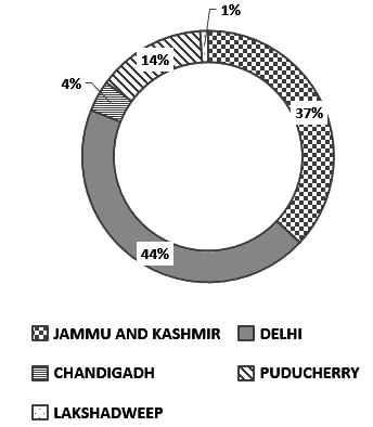
Delhi is what percent bigger than Chandigarh?
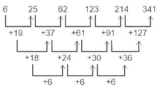
Complete the series choosing the missing number:
6, 25, 62, 123, 214, ______
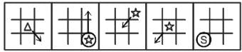
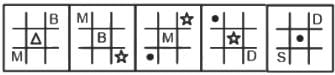
Select the figure from among the given options that can replace the question mark (?) in the following series.
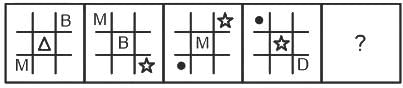
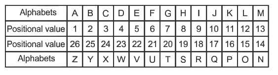
 is getting shifted and replaced with letter '
 .
.


Important Questions for ISRO Scientist Electronics Mock Test - 2
ISRO Scientist Electronics Mock Test - 2 MCQs with Answers
Online Tests for ISRO Scientist Electronics Mock Test - 2
|
© EduRev
|
Education Revolution
|


|


within 7 days!