Electronics and Communication Engineering (ECE) Exam  >  Electronics and Communication Engineering (ECE) Tests  >  ISRO Scientist Electronics Mock Test - 3 - Electronics and Communication Engineering (ECE) MCQ

ISRO Scientist Electronics Mock Test - 3 - Electronics and Communication Engineering (ECE) MCQ


Test Description

30 Questions MCQ Test - ISRO Scientist Electronics Mock Test - 3

ISRO Scientist Electronics Mock Test - 3 for Electronics and Communication Engineering (ECE) 2025 is part of Electronics and Communication Engineering (ECE) preparation. The ISRO Scientist Electronics Mock Test - 3 questions and answers have been prepared according to the Electronics and Communication Engineering (ECE) exam syllabus.The ISRO Scientist Electronics Mock Test - 3 MCQs are made for Electronics and Communication Engineering (ECE) 2025 Exam. Find important definitions, questions, notes, meanings, examples, exercises, MCQs and online tests for ISRO Scientist Electronics Mock Test - 3 below.
Solutions of ISRO Scientist Electronics Mock Test - 3 questions in English are available as part of our course for Electronics and Communication Engineering (ECE) & ISRO Scientist Electronics Mock Test - 3 solutions in Hindi for Electronics and Communication Engineering (ECE) course. Download more important topics, notes, lectures and mock test series for Electronics and Communication Engineering (ECE) Exam by signing up for free. Attempt ISRO Scientist Electronics Mock Test - 3 | 95 questions in 120 minutes | Mock test for Electronics and Communication Engineering (ECE) preparation | Free important questions MCQ to study for Electronics and Communication Engineering (ECE) Exam | Download free PDF with solutions
ISRO Scientist Electronics Mock Test - 3 - Question 1

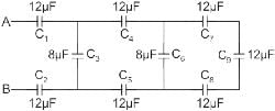
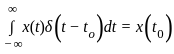
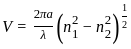
The total equivalent capacitance of the series parallel combination of capacitors across A and B shown in figure is

Detailed Solution for ISRO Scientist Electronics Mock Test - 3 - Question 1

Concept:
Equivalent capacitance of capacitors -
Connected in series: When n capacitors C1, C2, C3, ... Cn are connected in series, the net capacitance (Cs) is given by:

Connected in parallel: When n capacitors C1, C2, C3, ... Cn are connected in parallel, the net capacitance (Cp) is given by:
⇒ Cp = C1 + C2 + C3 +... Cn
Calculation:
C7, C9 and C8 are in series,
12 μF, 12 μF, 12 μF
Equivalent capacitance = (1/12) + (1/12) + (1/12) = 4 μF
4 μF is in parallel with 8 μF
Equivalent capacitance = (4 + 8) μF = 12 μF
C4, C5 are in parallel with 12 μF
Equivalent = 4 μF
C3 is in series with 8 μF
Total equivalent = 12 μF

C1 and C2 are parallel to 12 μF
Hence equivalent = 4 μF

ISRO Scientist Electronics Mock Test - 3 - Question 2

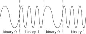
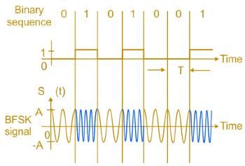
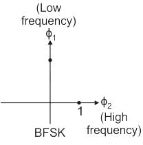
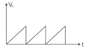
The given waveform describes operation of ______.

Detailed Solution for ISRO Scientist Electronics Mock Test - 3 - Question 2

BFSK (Frequency shift keying):
In FSK (Frequency Shift Keying) binary 1 is represented with a high-frequency carrier signal and binary 0 is represented with a low-frequency carrier, i.e. In FSK, the carrier frequency is switched between 2 extremes.

For binary ‘1’ → S1 (A) = Acos 2π fHt
For binary ‘0’ → S2 (t) = A cos 2π fLt . The constellation diagram is as shown:

ISRO Scientist Electronics Mock Test - 3 - Question 3

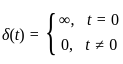
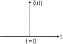
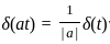
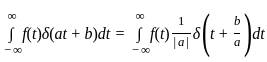
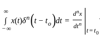
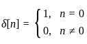
Which of the following points CANNOT be observed about a unit impulse function if it is assumed in the form of a pulse?

Detailed Solution for ISRO Scientist Electronics Mock Test - 3 - Question 3

Unit impulse signal:

It is defined as a pulse compressed along the horizontal axis and stretched along the vertical axis keeping the area unity.

It is defined as,

It exists only at t = 0 and the area under impulse function is unity.

Properties:

1.

2.

3. x(t) δ(t – t0) = x(t0)

4.

5.

6.

The discrete time version of the unit impulse is defined by

Properties:

1. x[n] δ[n] = x[0] δ[n]

2.

3. x[n] δ[n – n0] = x[n0] δ[n – n0]

4.

5. δ[an] = δ[n]

ISRO Scientist Electronics Mock Test - 3 - Question 4
If 
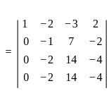
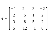
, then the rank of the matrix A is
Detailed Solution for ISRO Scientist Electronics Mock Test - 3 - Question 4

R1 → -R1

R2 → R2 - 2R1; R3 → R3 - 3R1; R4 → R4 - 5R1

R4 → R4 - 2R2; R3 → R3 - 2R2

So, r[A] = 2

ISRO Scientist Electronics Mock Test - 3 - Question 5
In a baseband communications link, frequencies upto 3500 Hz are used for signaling. Using a raised cosine pulse with 75% excess bandwidth and for no inter-symbol interference, the maximum possible signaling rate in symbols per second is
Detailed Solution for ISRO Scientist Electronics Mock Test - 3 - Question 5

Concept:

BT = 0.5 Rs(β + 1)

Rs → Symbol rate

Rs = (2 × βT)/(β + 1)

Calculations:

β = 0.75

Rs = (2 × 3500)/(0.75 + 1)

= 4000 symbols/sec

ISRO Scientist Electronics Mock Test - 3 - Question 6

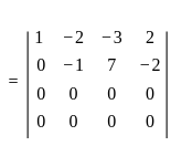
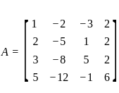
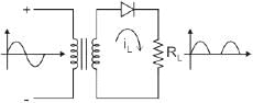
What is the output of a half wave rectifier (in V) when it is supplied with a voltage which has peak value of 12.5 V?

Detailed Solution for ISRO Scientist Electronics Mock Test - 3 - Question 6

Concept:
Half Wave Rectifier:

  • The basic circuit of a half-wave rectifier and its waveform with a resistive load is shown in Fig.
  • During the positive half-cycle of the input AC voltage, the diode is forward-biased (ON) and conducts.
  • While conducting, the diode acts as a short-circuit so that circuit current flows, and hence, a positive half-cycle of the input ac voltage is dropped across RL.
  • During the negative input half-cycle, the diode is reverse-biased (OFF) and so, does not conduct i.e. there is no current flow. Hence, there is no voltage drop across RL.

Consider Vm is the maximum value of Half wave rectifier,
∴ Average Value, Vav = Vm/π 
∴ RMS Value, VR Vm/2
Whenever output is asked simply we need to find out the average output value,
Calculation:
Vm = 12.5 V
Vav = 12.5/π = 4 V

ISRO Scientist Electronics Mock Test - 3 - Question 7

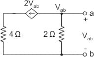
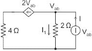
The Thevenin equivalent resistance (RTh) for the circuit shown in fig. is:

Detailed Solution for ISRO Scientist Electronics Mock Test - 3 - Question 7

To find the value of Rth:

By applying KCL we can find that,
I1 + 2Vab = I --- (1)
We can see that,
Vab = 2 I1
now, applying the value of Vab in equation 1, we get
0.5 Vab + 2 Vab = I
2.5 Vab = I

Rth = (Vab/I)
= 0.4 Ω

ISRO Scientist Electronics Mock Test - 3 - Question 8
Which of the following combination is representing an SCR?
Detailed Solution for ISRO Scientist Electronics Mock Test - 3 - Question 8
  • A silicon-controlled rectifier (SCR) is a four-layer solid state current controlling device with 3 terminals
  • The SCR combines the rectifying features of diodes and the on - off control features of transistors
  • SCRs are generally used in power switching applications
ISRO Scientist Electronics Mock Test - 3 - Question 9

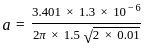
For a lossless transmission line L = 0.35 μH/m, C = 90 pF/m and frequency = 500 MHz. Then the magnitude of propagation constant is

Detailed Solution for ISRO Scientist Electronics Mock Test - 3 - Question 9

Concept:
The propagation constant of a transmission line is a complex quantity given by:
γ = α + jβ
α = Attenuation constant, related to the line parameters as:

β = Phase constant, related to the line parameters as:

For a loss lossless line, there is no attenuation, i.e. α = 0. The propagation constant will become:
γ = jβ
|γ| = |β|
Calculation:
Given:
L = 0.35 μH/m, C = 90 pF/m and frequency = 500 MHz
ω = 2πf = 2 × 3.14 × 500 × 106
ω = 3.142 × 10⁹ rad/sec
The magnitude of propagation constant for the given line will be:


|γ| ≈ 17.42
Important Point

Attenuation constant:

  • Attenuation constant gives attenuation of an electromagnetic wave propagating through a medium per unit distance from the source
  • It is the real part of the propagation constant and is measured in nepers per metre

Phase Constant:

  • The phase constant is the imaginary component of the propagation constant for a plane wave
  • It represents the change in phase per unit length along the path travelled by the wave at any instant
  • Phase constant is measured in radians per unit length
ISRO Scientist Electronics Mock Test - 3 - Question 10

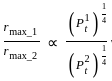
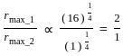
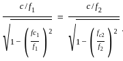
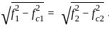
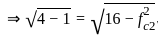
Two radars are transmitting powers P1 and P. If the transmitted power P1 is 16 times the transmitted power P2 and all other parameters are same then ratio of maximum range of radar 1 to radar 2 is:

Detailed Solution for ISRO Scientist Electronics Mock Test - 3 - Question 10

The maximum radar range is given by:

Where
Pt is the transmitted power
A0 is capture area
S = effective area
Pmin = minimum power at the receiver which can be recognized
λ = wavelength of EM radiation
rmax ∝ (Pt)4

ISRO Scientist Electronics Mock Test - 3 - Question 11

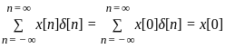
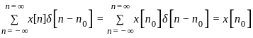
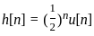
(u[n] is unit step pulses)

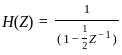
this system works as which type of filter?

Detailed Solution for ISRO Scientist Electronics Mock Test - 3 - Question 11

The correct answer is LPF

Concept:

Z = re

At low frequency ω = 0 we get Z = 1

At high frequency ω = π we get Z = -1

Solution:

Calculate the Z-transform of the given h[n]

at Z = 1 we get H(z) = 2

at Z = -1 we get H(z) = 2/3

as we can see we get a higher magnitude at low frequency hence this system will work as a Low pass filter.

ISRO Scientist Electronics Mock Test - 3 - Question 12

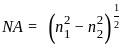
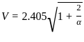
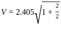
Find the maximum possible core diameter which allows single_mode operation at a wavelength of 1.3 μm in a graded-index fiber having a parabolic refractive index profile core with core refractive index at the core axis of 1.5 and relative index difference of 1%.

Detailed Solution for ISRO Scientist Electronics Mock Test - 3 - Question 12

Concept:

  • Optical fiber is a dielectric waveguide that operates in optical frequencies, normally in cylindrical form.
  • The inner cylindrical structure is core surrounded by the solid dielectric called cladding.
  • Variation in material composition gives rise to two commonly used fibers.
  • If the refractive index of fiber is uniform throughout and undergoes an abrupt change at the cladding boundary is called step-index fiber.
  • If the refractive index of fiber is varied as a function of radial distance from the center of the fiber is called graded-index fiber.

V number
It is a dimensionless number that is related to wavelength and numerical aperture and determines how many modes fiber can support and is given by.


Where,
n1 = refractive index of core
n2 = refractive index of cladding
a = radius of the core
λ = operating wavelength
Δ = Relative index difference of fiber and is given by

NA = numerical aperture of the fiber and is defined as
The numerical aperture of an optical fiber is a numerical value
it is the sine of the maximum possible launching angle of the optical fiber and is given by
NA = nsin(θ)


n = refractive index of medium from which light ray enter the fiber core
For lowest order or single-mode operation, V number is given by

α = various profile parameter of the fiber
α = 1 for triangular profile
α = 2 for parabolic profile
Calculation:
Given that
Operation wavelength (λ) = 1.3 μm
Core refractive index (n1) = 1.5
Relative index difference (Δ) = 0.01
α = 2 for parabolic profile
then


V = 2.405 × √2 = 3.401
We know that

The above equation can be rearranged as

Putting all values in the above equation

a = 3.316×10⁻⁶ meter
a = 3.316 μm
diameter of core (d) = 2a
d = 2 × 3.316 μm
d = 6.632 μm
Explanation
The number of modes for graded-index fiber is given by

α = various profile parameter of the fiber
α = 1 for triangular profile
α = 2 for parabolic profile

ISRO Scientist Electronics Mock Test - 3 - Question 13

Consider a closed surface S surrounding a volume V. If is the position vector of a point inside S, with the unit normal on S, the value of the integral is

Detailed Solution for ISRO Scientist Electronics Mock Test - 3 - Question 13

Concept:
The divergence theorem states that the surface integral of a vector field over a closed surface, which is called the flux through the surface, is equal to the volume integral of the divergence over the region inside the surface.
Calculation:
is the position vector of a point inside a closed surface.

= 5 x 3 = 15V

ISRO Scientist Electronics Mock Test - 3 - Question 14

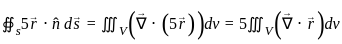
Consider a signal x (t) = 5 cos (2πt/3), + 9 sin (0.5π t) + 3 sin + 12. Identify the valid statement for x (t).

Detailed Solution for ISRO Scientist Electronics Mock Test - 3 - Question 14

Concept:
A continuous-time signal consisting of the sum of multiple time-varying functions is periodic, if and only if both functions are periodic and the ratio of these two periods is a rational number.
In such a case, the least common multiple(LCM) of those periods is the period of the sum signal.
Example:
x(t) = Acos(ω1t) + Bcos(ω2t) + Ccos(ω3​t)
Here
T1 = 2π/ω
1
T2 = 2π/ω2
T3 =
2π/ω3
Step 1: Check whether (T1/T2), (T2/T3), (T3/T1) rational or not.
If any of the ratio is not rational → Signal is nonperiodic
If ratios are rational → Signal is periodic and proceed to step 2

Step 2:
Common time period = LCM( T1, T2, T3)
Note : Addition of DC signal to periodic signal does hamper the periodicity
Calculation:
GIven;
x (t) = 5 cos (
2πt/3) + 9 sin (0.5π t) + 3 sin + 12
T1 = 2π/ω1 = 2π/(2π/3) = 3
T2 = 2π/ω2 = 2π/(0.5π) = 4
T3 = 2π/ω3 = 2π/(π/3) = 6
Here, (T1/T2), (T2/T3), (T3/T1) are rational
Common time period = LCM( T
1, T2, T3) = LCM( 3, 4, 6)= 12 sec
Frequency = 1/ Common time period = 1/12 Hz

Hence, x(t) is periodic with frequency (1/12) Hz

ISRO Scientist Electronics Mock Test - 3 - Question 15

An air-filled rectangular waveguide R1 is operating at the frequency 2 GHz and another air-filled rectangular waveguide R2 is operating at 4 GHz. The guide wavelengths of these waveguides at their respective frequencies are equal. If the cut-off frequency of waveguide R1 is 1 GHz, what is the cut-off frequency of the waveguide R2 in GHz?

Detailed Solution for ISRO Scientist Electronics Mock Test - 3 - Question 15

Calculation:
Guided wavelength is given by:
; where
fc = Cut-off frequency
And f = Operating frequency.
For waveguide R­1 : f1 = 2GHz and fc1 = 1 GHz
For waveguide R2 : f2 = 4 GHz. We are to find fc­2.
Given λg1 = λg2
Equating the wavelength for Both waveguides ;


⇒ 3 = 16 – fc22
fc22 = 13
fc2 = √13
Option (4) is the correct option.

ISRO Scientist Electronics Mock Test - 3 - Question 16

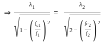
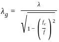
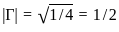
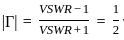
A lossless transmission line is terminated by a load which reflects a part of the incident power. If percentage of the power that is transmitted is 75%, what is value of VSWR is ______.

Detailed Solution for ISRO Scientist Electronics Mock Test - 3 - Question 16

Transmitted power = 75%

⇒ Reflected power = 25% = 1/4

Magnitude of reflection coefficient,

Also,

VSWR = 3

ISRO Scientist Electronics Mock Test - 3 - Question 17

Which of the following statements regarding Laplace and Fourier transforms are correct?
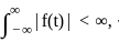
A. In order for a function to possess a Laplace transform, it must obey the condition 
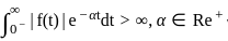
B. In order for a function to possess a Laplace transform, it must obey the condition
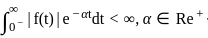
C. For a function to have a Fourier transform, it must obey the condition
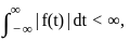
D. For a function to have a Fourier transform, it must obey the condition
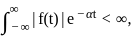
Choose the correct answer from the options given below:

Detailed Solution for ISRO Scientist Electronics Mock Test - 3 - Question 17

Concept:
The Fourier transform does not exist for all non-periodic signal.
And therefore, in order for a function x(t) to have Fourier transform, the following requirements, known as Dirichlet's conditions, must be satisfied
Function should be absolutely integrable form - to

Laplace Transform: It is an integral that converts real variable(usually time domain ) to a complex frequency domain (usually s domain)
In order to have Laplace Transform following criteria must be satisfied:

ISRO Scientist Electronics Mock Test - 3 - Question 18

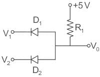
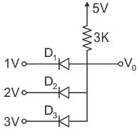
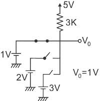
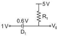
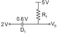
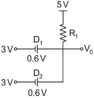
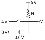
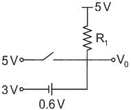
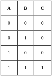
Consider the AND logic circuit in which V2 = 3 V and V1 lie between 0 to 5 V. The output voltage is V0. The cut-in voltage of diode D1 and D2 is 0.6 V. The output voltage V0 versus V1 corresponding to the below network is

Detailed Solution for ISRO Scientist Electronics Mock Test - 3 - Question 18

Concept:
Whenever diodes are tied together, the diode which experiences the more potential difference will ON first.

D3 is ON and remaining OFF.

When all diodes are opposite to the previous case.

D1 is ON and remaining OFF

If all are given the same voltage then all will be ON

Calculation:
Given voltage levels are V1 = 0 to 5 V and V2 = 3V
Until V1 < 3 V diode D2 is OFF
For V1 = 1 V

V0 = 1.6 V
For V2 = 2 V

V0 = 2.6 V
For V1 = 3 V
Both will be ON

V0 = 3.6 V
For V1 = 4 V diode D1 will be OFF.

V0 = 3.6 V
For V1 = 5 V diode D1 will be OFF.

V0 = 3.6 V
So the output is constant at 3.6 V for V1 ≥ 3 V
Option B is correct.

ISRO Scientist Electronics Mock Test - 3 - Question 19
A signal x(t) = 100 cos (24 π × 103t) is ideally sampled with a sampling period of 50 μsec and then passed through an ideal lowpass filter with a cut-off frequency of 15 kHz. Which of the following frequencies will be present at the filter output:
Detailed Solution for ISRO Scientist Electronics Mock Test - 3 - Question 19

Calculation:

Given, message signal x(t) = 100 cos (24 π × 103t)

Sampling period, Ts = 50 μsec

So, we have the sampling frequency

Also, the frequency of the message signal fm is:

Clearly, the sampling frequency (fs) is less than the minimum Nyquist sampling frequency of 2fm.

So, the output will contain frequency components of:

fm ± nfs, where n = 0, 1, 2 …

For the given signal, we have the frequency components of the sampled output as:

fm = 12 kHz

fs + fm = 20 + 12k = 22 kHz

fs – fm = 20 – 12 k = 8 kHz

2fs + fm = 40 + 12 = 52 kHz

2fs – fm = 40 – 12 = 28 kHz and so on.

When these signal components are passed through a low pass filter with cut-off frequency fc = 15 kHz, we get the output with frequency components:

fm = 12 kHz and fs – fm = 8 kHz.
ISRO Scientist Electronics Mock Test - 3 - Question 20

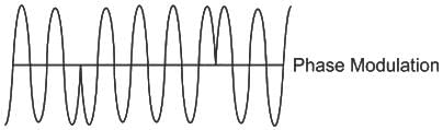
For a given frequency deviation in FM modulation, the modulation index varies______.

Detailed Solution for ISRO Scientist Electronics Mock Test - 3 - Question 20

Concept:
In FM (Frequency Modulation), the modulation index is defined as the ratio of frequency deviation to the modulating frequency.
Mathematically, this is defined as:
mf = Δf/fm
mf = Modulation index
Δf = Frequency deviation
fm = Modulating frequency
We observe that the modulation index for FM signal is inversely proportional to the modulating frequency fm.
Important Point
A wave has 3 parameters Amplitude, Phase, and Frequency. Thus there are 3 types of modulation techniques.
Amplitude Modulation: The amplitude of the carrier is varied according to the amplitude of the message signal.
Frequency Modulation: The frequency of the carrier is varied according to the amplitude of the message signal.
Phase Modulation: The Phase of the carrier is varied according to the amplitude of the message signal.


ISRO Scientist Electronics Mock Test - 3 - Question 21

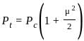
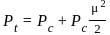
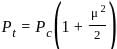
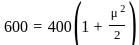
If the total power of an amplitude modulated signal is 600 W and the carrier power is 400 W, the modulation index is

Detailed Solution for ISRO Scientist Electronics Mock Test - 3 - Question 21

Concept:
The total transmitted power for an AM system is given by:

Pc = Carrier Power
μ = Modulation Index
The above expression can be expanded to get:

The total power is the sum of the carrier power and the sideband power, i.e.

Calculation:
Given Pt = 600 W, Pc = 400 W
We can write:


(1.5 - 1) × 2 = μ2
μ = 1

ISRO Scientist Electronics Mock Test - 3 - Question 22

Refer to the code given below, which kind of circuit is implemented?
PROCESS
BEGIN
WAIT ON
X, Y;
Z < = X and Y;
END PROCESS;

Detailed Solution for ISRO Scientist Electronics Mock Test - 3 - Question 22

Sequential circuit
This is represented when the process has the clock signal in its sensitivity list else we can’t call that a sequential circuit.
Since the given process doesn’t have any clock signal. So, it can’t be a sequential circuit and hence the process is a combinational circuit.
WAIT statement also only one and this represents the given circuit is sequential.
An example of sequential circuit code is represented below:
entity d_ff is port ( CLK, d: in bit; q: out bit ) ;
end d_ff ;
architecture rtl of d_ff is
begin
process(CLK)
begin
if clk’event and clk = ’1’
then q <= d ;
end if ;
end process ;
end rtl ;

Conclusion:
The given circuit is a combinational circuit.

ISRO Scientist Electronics Mock Test - 3 - Question 23

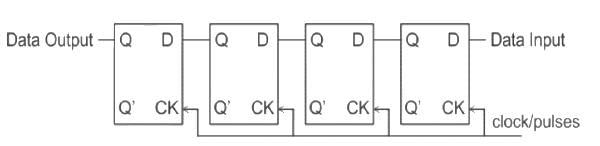
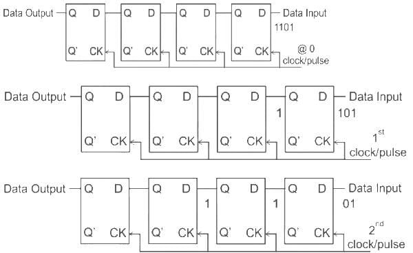
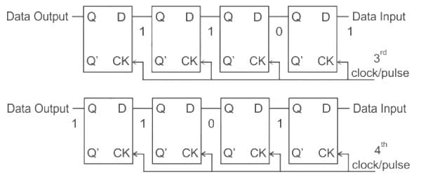
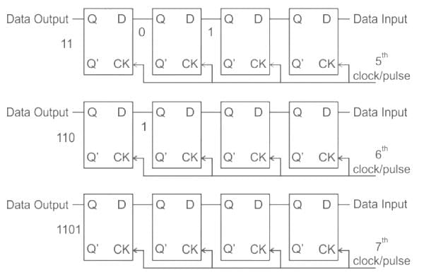
What is the number of clock pulses required to completely load and then unload a 4-bit register?

Detailed Solution for ISRO Scientist Electronics Mock Test - 3 - Question 23

Concept:

  • Shift Registers are sequential logic circuits, capable of storage and transfer of data.
  • They are made up of Flip Flops which are connected in such a way that the output of one flip flop could serve as the input of the other flip-flop, depending on the type of shift registers being created.
  • Shift registers are a type of register that has the ability to transfer (“shift”) data.
  • Registers are storage devices that are created by connecting a specific number of flip flops in series.
  • The number of bits that can be stored by the register is always directly proportional to the number of flip flops ( as each flip flop is capable of storing only one bit at a time).
  • The number of clock pulses needed to load and unload an n-bit shift register will be (2n – 1).


To load a 4-bit binary number 1101 in a register, it will take 4 clock pulses.

Example: Let 1101 is the input to a shift register. The working of the register after each clock pulse is as shown:

After the 4th clock pulse, all the bits are stored in each flip-flop of the register. We can observe that one bit is already at the output terminal.

∴ It will require another 3 clock pulses to get the other three bits at the output terminal, i.e. it requires 7 clock pulses to load and unload the 4-bit register.

This is as shown:

ISRO Scientist Electronics Mock Test - 3 - Question 24

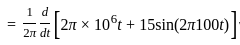
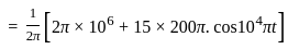
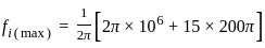
A signal m(t) = 10 cos (2π 100t) is frequency-modulated. The resulting FM signal is x(t) = 20 cos {2π 106 t + 15 sin (2π 100 t)}

The FM bandwidth is nearly
Detailed Solution for ISRO Scientist Electronics Mock Test - 3 - Question 24

Concept:

According to Carson rule signal, BW is given as:

B.W = (β + 1) 2fm

B.W. = 2[Δf + fm]

If multiple frequencies are available in modulating signal then,

B.W. = 2(β + 1) fmax

Calculation:

Given:

m(t) = 10 cos (2π 100t)

The resulting FM signal is given as:

x(t) = 20 cos {2π 106 t + 15 sin (2π 100 t)}

The instantaneous frequency is given by:

Maximum instantaneous frequency

Maximum frequency deviation

= 1.5 kHz

Given, fm = 100 Hz = 0.1 kHz

So, Approximate bandwidth according to Carson’s rule

⇒ 2(Δf + fm)

= 2(1.5 + 0.1)

= 2 (1.6 k)

= 3.2 kHz

ISRO Scientist Electronics Mock Test - 3 - Question 25

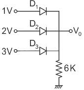
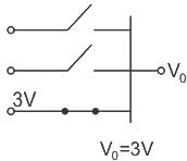
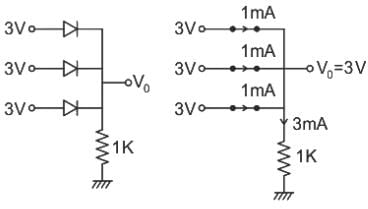
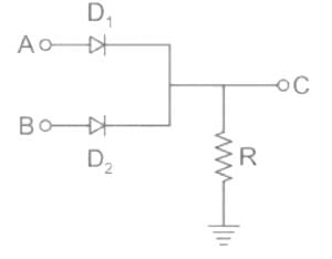
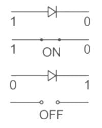
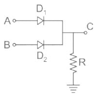
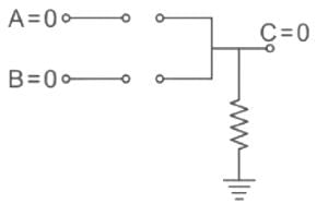
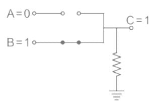
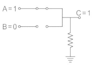
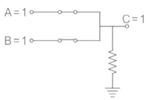
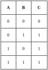
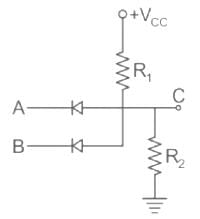
Which of the following logical operations could be computed by the given network?

Detailed Solution for ISRO Scientist Electronics Mock Test - 3 - Question 25

Concept:
In Digital Electronics, Logic 1 means High and Logic 0 means low.
Whenever in diode, if 1 is applied to anode and 0 to cathode then Diode acts as a short circuit i.e. ON.
And if 0 is applied to anode and 1 to cathode Diode acts as open circuit i.e. OFF.

Explanation:
The given logic circuit is

For different logic of A and B,4 cases are there and according to that logic of C will vary.

Case 1
When A is logic 0 and B is logic 0

Then the logic of C will be 0.

Case 2
When A is logic 0 and B is logic 1


Then the logic of C will be 1.

Case 3
When A is logic 1 and B is logic 0

Then the logic of C will be 1.

Case 4
When A is logic 1 and B is logic 1

Then the logic of C will be 1.
According to Result, we make a table

This Table is of Logic OR gate.
C = A + B

Important PointsLogic Circuit for AND gate is C = AB

ISRO Scientist Electronics Mock Test - 3 - Question 26

In root-locus plot, the breakaway points

Detailed Solution for ISRO Scientist Electronics Mock Test - 3 - Question 26

Concept:
1. Every branch of a root locus diagram starts at a pole (K = 0) and terminates at a zero (K = ∞) of the open-loop transfer function.
2. The root locus diagram is symmetrical with respect to the real axis.
3. A number of branches of the root locus diagram are:
N = P if P ≥ Z
= Z, if P ≤ Z
4. Number of asymptotes in a root locus diagram = |P – Z|
5. Centroid: It is the intersection of the asymptotes and always lies on the real axis. It is denoted by σ.

ΣPi is the sum of real parts of finite poles of G(s)H(s)
ΣZi is the sum of real parts of finite zeros of G(s)H(s)
6. The angle of asymptotes:
l = 0, 1, 2, … |P – Z| – 1
7. On the real axis to the right side of any section, if the sum of the total number of poles and zeros are odd, the root locus diagram exists in that section.
8. Break-in/away points: These exist when there are multiple roots on the root locus diagram.
At the breakpoints gain K is either maximum and/or minimum.
So, the roots of dK/ds are the breakpoints.

Observation:
n root-locus plot, the breakaway points, must lie on the root loci.

ISRO Scientist Electronics Mock Test - 3 - Question 27

A blocking oscillator is a _________

Detailed Solution for ISRO Scientist Electronics Mock Test - 3 - Question 27

  • A blocking oscillator used to produce narrow pulses or trigger pulses it is also called Saw-tooth wave oscillator
  • When we take feedback from the output signal, it blocks the feedback, after a cycle, for certain predetermined time
ISRO Scientist Electronics Mock Test - 3 - Question 28

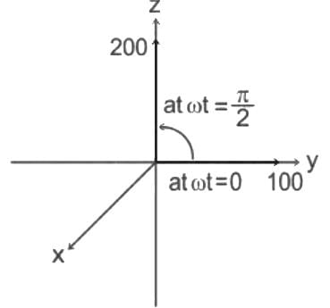
The electric field intensity of the wave is given as

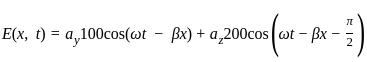
The polarization of the wave is:

Detailed Solution for ISRO Scientist Electronics Mock Test - 3 - Question 28

Concept:
The polarization of a plane wave is the “figure traced by the tip of the electric field vector as a function of time, at a fixed point in space.”

Calculation:
The given wave can be written as;
⇒ E(x, t) = ay 100 cos (ωt - βx) + az 200 sin (ωt - βx)
Fixing a point, i.e. x = 0
⇒ E (0, t) = ay 100 cos (ωt) + az 200 sin (ωt)
When, ωt = 0
E = ay (100)


E = az (200)
This can be explained as:
Since the magnitude of ‘y’ and ‘z’ components are unequal and the tip of the field is rotating in the counter-clockwise direction. The polarization is right-hand elliptical polarization. So, option (B).

ISRO Scientist Electronics Mock Test - 3 - Question 29

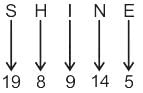
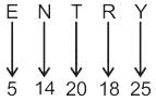
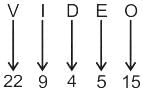
In a certain code language, 'SHINE' is written as '11', and 'ENTRY' is written as '16.4'. How will 'VIDEO' be written in that language?

Detailed Solution for ISRO Scientist Electronics Mock Test - 3 - Question 29
The positional value table is as follows:

The pattern followed here is:

Code = Sum of positional values of letters ÷ Number of letters in the word.

  • In SHINE → 11

  • Code = Sum of positional values of letters ÷ Number of letters in the word
  • Code = (19 + 8 + 9 + 14 + 5) ÷ 5
    = 55 ÷ 5
    = 11​​​
  • In ENTRY → 16.4 ​

  • Code = Sum of positional values ÷ Number of letters in the word
  • Code = (5 + 14 + 20 + 18 + 25) ÷ 5
    = 82 ÷ 5
    = 16.4
  • Similarly, In VIDEO → ​

  • Code = Sum of positional values ÷ Number of letters in the word
  • Code = (22 + 9 + 4 + 5 + 15) ÷ 5
    = 55 ÷ 5
    = 11.​​​

We get '11'.
Hence, "Option 3" is the correct answer.

ISRO Scientist Electronics Mock Test - 3 - Question 30

Select the number which is different from the others.

Detailed Solution for ISRO Scientist Electronics Mock Test - 3 - Question 30

The logic followed here is → (First digit of the first number × Second digit of the first number) + (Sum of the digits of first number) = Second number

So,
Option - (1) → 68 - 62
⇒ (6 × 8) + (6 + 8) = 62
⇒ 48 + 14 = 62
⇒ 62 = 62 (LHS = RHS)

Option - (2) → 72 - 23
⇒ (7 × 2) + (7 + 2) = 23
⇒ 14 + 9 = 23
⇒ 23 = 23 (LHS = RHS)

Option - (3) → 35 - 22
⇒ (3 × 5) + (3 + 5) = 22
⇒ 15 + 8 = 22
⇒ 23 22 (LHS RHS)

Option - (4) → 91 - 19
⇒ (9 × 1) + (9 + 1) = 19
⇒ 9 + 10 = 19
⇒ 19 = 19 (LHS = RHS)
Here, "35 - 22" is different from rest of the alternatives.
Hence, "Option - (3)" is the correct answer.

View more questions
Information about ISRO Scientist Electronics Mock Test - 3 Page
In this test you can find the Exam questions for ISRO Scientist Electronics Mock Test - 3 solved & explained in the simplest way possible. Besides giving Questions and answers for ISRO Scientist Electronics Mock Test - 3, EduRev gives you an ample number of Online tests for practice
Download as PDF