Electrical Engineering (EE) Exam > Electrical Engineering (EE) Tests > GATE Electrical Engineering (EE) Mock Test Series 2026 > Test: Semiconductor Diodes - Electrical Engineering (EE) MCQ
Test: Semiconductor Diodes - Electrical Engineering (EE) MCQ
Test Description
10 Questions MCQ Test GATE Electrical Engineering (EE) Mock Test Series 2026 - Test: Semiconductor Diodes
Test: Semiconductor Diodes for Electrical Engineering (EE) 2025 is part of GATE Electrical Engineering (EE) Mock Test Series 2026 preparation. The Test: Semiconductor Diodes questions and answers have been
prepared according to the Electrical Engineering (EE) exam syllabus.The Test: Semiconductor Diodes MCQs are made for Electrical Engineering (EE) 2025 Exam. Find important
definitions, questions, notes, meanings, examples, exercises, MCQs and online tests for Test: Semiconductor Diodes below.
Solutions of Test: Semiconductor Diodes questions in English are available as part of our GATE Electrical Engineering (EE) Mock Test Series 2026 for Electrical Engineering (EE) & Test: Semiconductor Diodes solutions in
Hindi for GATE Electrical Engineering (EE) Mock Test Series 2026 course. Download more important topics, notes, lectures and mock
test series for Electrical Engineering (EE) Exam by signing up for free. Attempt Test: Semiconductor Diodes | 10 questions in 30 minutes | Mock test for Electrical Engineering (EE) preparation | Free important questions MCQ to study GATE Electrical Engineering (EE) Mock Test Series 2026 for Electrical Engineering (EE) Exam | Download free PDF with solutions
Test: Semiconductor Diodes - Question 1
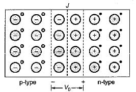
The barrier voltage (V0 or Vr) in a junction diode is the effect of
Detailed Solution for Test: Semiconductor Diodes - Question 1
Detailed Solution for Test: Semiconductor Diodes - Question 2
Detailed Solution for Test: Semiconductor Diodes - Question 3
Test: Semiconductor Diodes - Question 4
The most commonly used type of electron emission in electron tubes is
Detailed Solution for Test: Semiconductor Diodes - Question 5
Test: Semiconductor Diodes - Question 6
The emission of electrons in a vacuum diode is achieved by
Test: Semiconductor Diodes - Question 7
The main reason why electrons can tunnel through a p-n junction is that
Detailed Solution for Test: Semiconductor Diodes - Question 7
Detailed Solution for Test: Semiconductor Diodes - Question 8
Test: Semiconductor Diodes - Question 9
The barrier voltage for germanium is _________ at 25°C.
Detailed Solution for Test: Semiconductor Diodes - Question 9
Test: Semiconductor Diodes - Question 10
With the increase in temperature, the resistivity of an intrinsic semiconductor decreases. This is because, with the increase of temperature
Detailed Solution for Test: Semiconductor Diodes - Question 10
|
26 docs|257 tests
|
Information about Test: Semiconductor Diodes Page
In this test you can find the Exam questions for Test: Semiconductor Diodes solved & explained in the simplest way possible.
Besides giving Questions and answers for Test: Semiconductor Diodes, EduRev gives you an ample number of Online tests for practice
|
26 docs|257 tests
|
Download as PDF


