Electronics and Communication Engineering (ECE) Exam  >  Electronics and Communication Engineering (ECE) Tests  >  GATE ECE (Electronics) Mock Test Series 2025  >  Test: BJT Construction & Operation - Electronics and Communication Engineering (ECE) MCQ

Test: BJT Construction & Operation - Electronics and Communication Engineering (ECE) MCQ


Test Description

10 Questions MCQ Test GATE ECE (Electronics) Mock Test Series 2025 - Test: BJT Construction & Operation

Test: BJT Construction & Operation for Electronics and Communication Engineering (ECE) 2025 is part of GATE ECE (Electronics) Mock Test Series 2025 preparation. The Test: BJT Construction & Operation questions and answers have been prepared according to the Electronics and Communication Engineering (ECE) exam syllabus.The Test: BJT Construction & Operation MCQs are made for Electronics and Communication Engineering (ECE) 2025 Exam. Find important definitions, questions, notes, meanings, examples, exercises, MCQs and online tests for Test: BJT Construction & Operation below.
Solutions of Test: BJT Construction & Operation questions in English are available as part of our GATE ECE (Electronics) Mock Test Series 2025 for Electronics and Communication Engineering (ECE) & Test: BJT Construction & Operation solutions in Hindi for GATE ECE (Electronics) Mock Test Series 2025 course. Download more important topics, notes, lectures and mock test series for Electronics and Communication Engineering (ECE) Exam by signing up for free. Attempt Test: BJT Construction & Operation | 10 questions in 30 minutes | Mock test for Electronics and Communication Engineering (ECE) preparation | Free important questions MCQ to study GATE ECE (Electronics) Mock Test Series 2025 for Electronics and Communication Engineering (ECE) Exam | Download free PDF with solutions
Test: BJT Construction & Operation - Question 1

Which of the following is not a valid type of BJT?

Detailed Solution for Test: BJT Construction & Operation - Question 1

A BJT is a device with a layer of semiconductor sandwiched between 2 unlike types of semiconductors and hence, PPN is not a valid type of a BJT.

Test: BJT Construction & Operation - Question 2

In a BJT, which of the following layers is heavily doped?

Detailed Solution for Test: BJT Construction & Operation - Question 2

The emitter is the most heavily doped and contains the maximum amount of charge carriers. It is the emitter’s task to inject carriers into the base. These bases are thin and lightly doped. For npn B JT, emitter injects electrons, and for pnp, it injects holes.

1 Crore+ students have signed up on EduRev. Have you? Download the App
Test: BJT Construction & Operation - Question 3

What is the typical order of magnitude of the base current for a BJT?

Detailed Solution for Test: BJT Construction & Operation - Question 3

As the base current is quite lower as compared to the collector and emitter current, it is usually in the order of microamperes.

Test: BJT Construction & Operation - Question 4

Which of the following currents in a BJT is also called leakage current?

Detailed Solution for Test: BJT Construction & Operation - Question 4

Leakage current in BJT is represented by ICO, which is due to the flow of minority carriers in the transistor. It consists of ICBO and ICEO. ICO depends on temperature, doubling with 10° rise in temperature. It thus effects total collector current, IC, and hence affects the power dissipation.

Test: BJT Construction & Operation - Question 5

Which of the following relations are correct?

Detailed Solution for Test: BJT Construction & Operation - Question 5

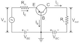
On applying KCL to the BJT, we get IC + IB = IE.

Test: BJT Construction & Operation - Question 6

Considering the resistances of emitter, collector and base to be Re, Rc and Rb respectively, which of the following is the correct statements?

Detailed Solution for Test: BJT Construction & Operation - Question 6

As the base is lightly doped, the number of free charge carriers are less and hence the resistance is high and as the emitter is the most highly doped, its resistance is low.

Test: BJT Construction & Operation - Question 7

For a BJT, what is typically the shape of the power dissipation curve, if it’s plotted on the output characteristics?

Detailed Solution for Test: BJT Construction & Operation - Question 7

ower Dissipation in a BJT is given by P=VCE.IC. This is in the form of k=xy which is the equation of a hyperbola.

Test: BJT Construction & Operation - Question 8

If the positive lead of a DMM, with the mode set to ohmmeter is connected to the base and the negative lead to the emitter and a low resistance reading is obtained, then what is the type of transistor that is being tested?

Detailed Solution for Test: BJT Construction & Operation - Question 8

There are multiple ways to test the BJT to be npn or pnp using a DMM based upon which terminals are connected to which lead of the DMM. If positive is to base and negative to the emitter of the BJT, and if a low reading is obtained and not a over limit, then the transistor is NPN.

Test: BJT Construction & Operation - Question 9

An enhancement type NMOS transistor with V1 = 0.7 V and source terminal grounded and 1.5 V applied to the gate. In what region does the device operate for VD = 0.5 V?

Detailed Solution for Test: BJT Construction & Operation - Question 9

Concept:

For an NMOS transistor If;

VGS > V and VDS < (VGS - VT) → Device is in Triode region

VGS > VT  and VDS ≥  (VGS - VT) → Device is in the Saturation region

Analysis:

Given;

Vt = 0.7 V

VS = 0 V

VG = 1.5 V

VD = 0.5 V

VGS = VG - VS = 1.5 - 0 = 1.5V

VDS = VD - VS =0.5 - 0 = 0.5 V

As, VDS < (VGS - VT)

The device will be in Triode region'

Test: BJT Construction & Operation - Question 10

Which of the following parameters will be very high in the common base configuration of a bipolar junction transistor?

Detailed Solution for Test: BJT Construction & Operation - Question 10

Common Base Configuration of BJT:

  • In the Common base configuration, the base connection is common to both the input signal AND the output signal.
  • The input signal is applied between the transistors base and the emitter terminals, while the corresponding output signal is taken from between the base and the collector terminals.
  • The base terminal is grounded or can be connected to some fixed reference voltage point.

Characteristics of Common base BJT:

  • Input Impedance - Low
  • Output Impedance - Very High
  • Phase Shift - 0o
  • Voltage Gain - High
  • Current Gain - Low
  • Power Gain - Low
25 docs|263 tests
Information about Test: BJT Construction & Operation Page
In this test you can find the Exam questions for Test: BJT Construction & Operation solved & explained in the simplest way possible. Besides giving Questions and answers for Test: BJT Construction & Operation, EduRev gives you an ample number of Online tests for practice

Top Courses for Electronics and Communication Engineering (ECE)

Download as PDF

Top Courses for Electronics and Communication Engineering (ECE)