Analyzing Delay in few Sequential Circuits - Electrical Engineering (EE) PDF Download

Objectives
In this lecture you will learn the delays in following circuits
- S-R Latch using NOR Gates
- Simple Latch using two Inverters (Bistable Element)
- Motivation
- Negative D-Latch
- Master Slave Flip-Flop
20.1 Motivation
We know that digital circuits are formed by two type of components- (1) Combinational circuit and (2) Sequential Circuits. Combinational circuit components are used only for logic implementation and can' t store the bits i.e. work as memory. But Sequential circuit components can store bits, hence used as memory elements. How fast a circuit (containing memory elements i.e sequential elements) can store or retrieve the value from its memory depends upon the delays in each of such basic sequential elements e.g. flip-flops etc.
In coming sections, We will analyze basic functionalities and delays of such sequential elements-
20.2 Negative D-Latch
Structure: This circuit consist of a multiplexer and an inverter . Data is fed at the i1 input of mux where as the output is given to
the inverter, which in turn is fed to the i2 input of the mux. Clock is given to the select input.
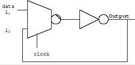
Fig 20.2 Negative D-Latch Circuits
Working:
When clock = '0' the data is passed on to the output.
When clock = '1' the data gets latched.
This circuit can be converted into positive clock latch by giving an inverted clock at the select input.
Note: Latch = level senstive Flip flop = edge triggered.
20.3 S-R Latch using NOR Gates
Structure: Using two nor gates this circuit is designed .In this circuit one of the input of nor gate is 'R' .Other input is 
Truth Table:
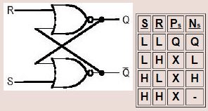
Fig 20.3: S-R Latch circuits using NOR
and the output of the gate is Q. In the second NOR gate the inputs are S and and the output is Q. Thus we see that the two inputs are connected in feedback configuration.
Note: Synchronous circuit: A circuit is said to be in synchronous mode if the output data speed is equal to the speed of the clock.
Asynchronous circuit: A circuit is said to be in asynchronous mode
if the output data speed is less than the speed of the clock.
Setup time: it is the time for which the valid data must be present before the clock edge arrives.
Hold time: it is the time for which the data must be held after the arrival of the clock edge. Sufficient set up and hold time must be provided to prevent contention of data.
20.4 Simple Latch using two Inverters (Bistable Element)
Structure: Here the output voltage of ig1 is equal to the input of ig2, and vice-versa. Fig 20.41 show the latch using two inverters.
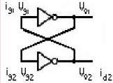
Fig 20.41: Latch using two inverters
Working: Notice that the input and output voltages of ig2 correspond to the output and input voltages of ig1 respectively. It can be seen that the two voltage transfer characteristics intersect at three points. Two of them are stable, while the middle point is unstable. The gain at the stable points is less than unity. Thus if input is at any of these points, it remains stable. The voltage gain at the third operating point is greater than unity. However if the input has a small perturbation, it is amplified and led to any of the two stable states. Hence this state is called metastable state. Since the circuit has two stable operating points it is called bistable. The potential energy is at its minimum at two of the three operating points, since the voltage gains of both inverters are equal to zero. By contrast, energy attains maximum value at the operating point at which the voltage gains of both inverters are maximum. Thus the circuit has two stable states corresponding to the two energy minima, and one unstable state corresponding to the potential energy maximum.
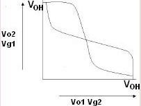
Fig 20.42: Stability Graph
Consider the above circuit at vg1 =vg2=vinv, the unstable operating point. Assume that
input capacitance cg of each inverter is much more than output capacitance cd. The drain current of each inverter is also equal to the gate current of other inverter.

where gm represents transconductance of inverter.. The gate charges q1 and q2 are -
The small signal gate current of each inverter can be written as-

Using eq1 and eq3,

These equation In terms q1 & q2 is given as below-
Combining equations eq5 and eq6, we will get
This expression is simplified by using To, the transient time constant
The time domain solution is 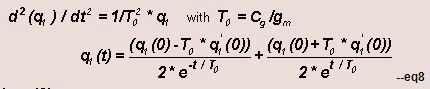
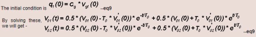
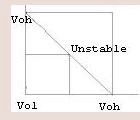
Fig 20.3: Voltage Stablity graph
Note that the magnitude of both the output voltages increases exponentially with time. Depending on the polarity of the initial small perturbation dVo1(0) and dVo2(0) the output voltages will diverge from there initial value of Vinv to either Vol or Voh
Solution for the problem:
1. The inverter should not be identical.
2. The lines connecting the two inverters should be of different lengths.
Note: 1.this same circuit can be used as static ram. After the data which is fed has started circulating, the input can be removed since it keep on circulating.
2. This circuit is also called as transparent latch or level sensitive latch.
20.4 Master Slave Flip-Flop or 1-bit shift resister (d negative edge triggered flip flop)
1: When the clock is at logic low the pass gate no.1 of master allows the input to pass the input to its output
2: when the clock is at logic high pass gate no.2 of master becomes transparent and the input gets latched.
3: In the second part, when the clock is at logic high the slave passes the output of master which was initially inverted to its output by again inverting it. Thus the input data D reaches the output at negative edge of the clock cycle.
4: If the clock is low, then the slave part latches the output.
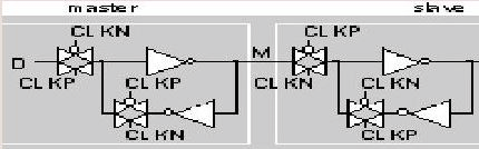
Fig 20.41: Master Slave Flip-Flop circuit
Another circuit for Negative Edge Triggered D flip/flop:
Advantage In this circuit is we need to use just 8 transistors.
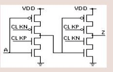
Fig 20.42: Alternative circuit of Master Slave Flip-Flop
Working: When the clock input is low, then the output is in high impedance state. So we are not able to get any data at the output. So the earlier data which was stored at the output capacitance is latched. In the next clock phase, the output terminal is connected to the pull-down or pull-up networks. So the data which is at input of the pull-down or pull-up network is stored at output in its inverted form. In the second part of the circuit the same process takes place. Thus the data is shifted by a bit, and acts as a 1-bit shift register.
Disadvantage: 1) There is a problem of charge sharing in this circuit.
2) This is used for slower circuits. Note: Clock frequency <= 1/(5*propagation delay).
FAQs on Analyzing Delay in few Sequential Circuits - Electrical Engineering (EE)
| 1. What is delay in sequential circuits? |  |
| 2. How does delay affect the performance of sequential circuits? | |
| 3. What are the factors that contribute to delay in sequential circuits? | |
| 4. How is delay calculated in sequential circuits? | |
| 5. How can delay in sequential circuits be minimized? | |


Summary
,shortcuts and tricks
,Previous Year Questions with Solutions
,Semester Notes
,Viva Questions
,video lectures
,Analyzing Delay in few Sequential Circuits - Electrical Engineering (EE)
,Important questions
,Sample Paper
,Exam
,Analyzing Delay in few Sequential Circuits - Electrical Engineering (EE)
,study material
,MCQs
,mock tests for examination
,Analyzing Delay in few Sequential Circuits - Electrical Engineering (EE)
,past year papers
,Extra Questions
,ppt
,practice quizzes
,Objective type Questions
,Free
;


Analyzing Delay in few Sequential Circuits Free PDF Download
Importance of Analyzing Delay in few Sequential Circuits
Analyzing Delay in few Sequential Circuits Notes
Analyzing Delay in few Sequential Circuits Electrical Engineering (EE) Questions
Study Analyzing Delay in few Sequential Circuits on the App
|
© EduRev
|
Education Revolution
|


|


