Bipolar Junction Transistor Amplifiers | Analog and Digital Electronics - Electrical Engineering (EE) PDF Download
| Table of contents |

|
| Amplifier Module |

|
| Different Amplifier Configurations |

|
| Common Base Amplifier Circuit |

|
| Common Collector Amplifier |

|
| Common Emitter Amplifier |

|
| Common Emitter Amplifier Example |

|
An Amplifier circuit is used to increase the strength of the signal. The amplifier circuit uses the power supply to increase the signal strength. The amplification provided by the amplifier circuit is measured in terms of Gain of an amplifier. The gain of the amplifier is the ratio of output to input, which is always greater than one. Amplification does not alter frequency and waveform shape.
Gain of the Amplifier (A) = Output/(Input)
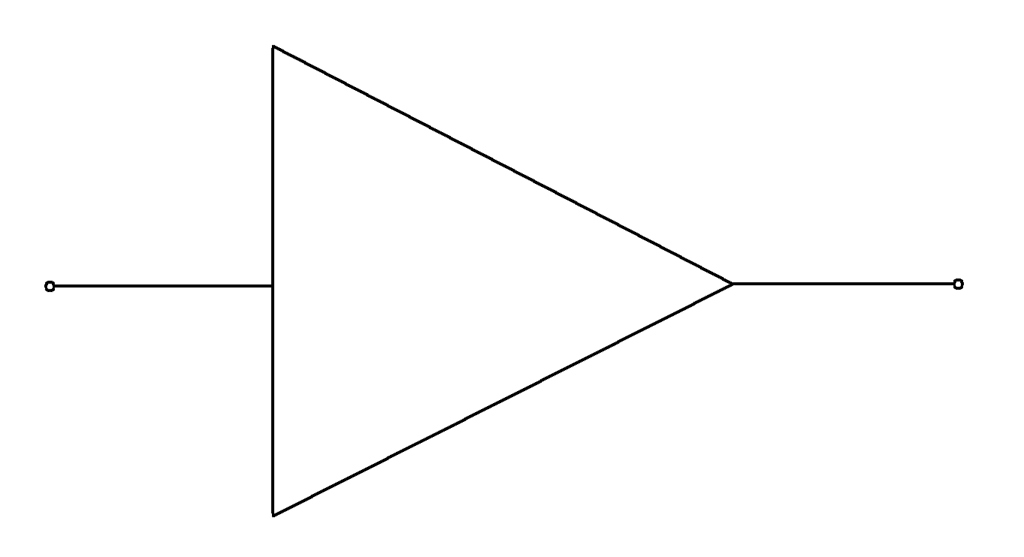 Symbol for Amplifier
Amplifier Module
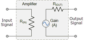
The ideal amplifier module has three important properties, namely, input impedance (Rin), output impedance (Rout) and of course amplification called as Gain(A). The amplifier module explains the general system of amplification with input and output signal. The impedance Rin increases the signal strength at gain A to produce the desired signal strength. Rin should be infinite and Rout should be zero.
Different Amplifier Configurations
Transistors are used in amplifiers in three different configurations, namely,
- Common Base (CB)
- Common Collector (CC)
- Common Emitter (CE).
The Common Emitter circuit is most widely used configuration. This circuit has grounded emitter. This circuit gives a medium level input impedance and output impedance. Voltage gain and current gain are medium, and the output reverses the input.
The Common collector circuit is widely used as a buffer. It is called as Emitter-follower. The emitter voltage follows that of the base. This gives a high input impedance and low output impedance. It has grounded collector.
The Common base circuit provides low input impedance and high output impedance. The base of the transistor in this configuration is grounded. Input and output are in phase.
Common Base Amplifier Circuit
NPN and PNP transistors are used in Amplifier circuits. Both NPN and PNP have input provided at the emitter of the transistor and the output is taken at the collector of the transistor.
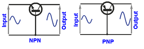 Common Base Amplifier Configuration
The below diagram shows how common base amplifier circuit is implemented.
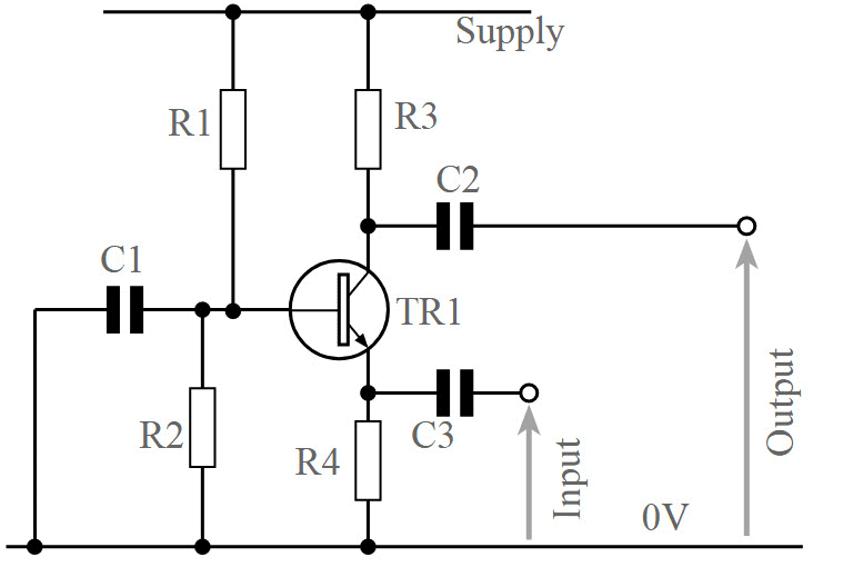
The biasing constraints are same, but the applications of the signals are different. In this circuit, care has to be taken such that correct impedance match is provided to the input signal.
Characteristics of Common Base Amplifier Circuit
The following are the characteristics of the Common Base amplifier circuit.
- High voltage gain
- Low current gain
- Low power gain
- Input and output phase relation is 0o
- It has low input impedance
- It has high output impedance
Common Collector Amplifier
The Common Collector Amplifier is another type of bipolar junction transistor, (BJT) configuration where the input signal is applied to the base terminal and the output signal taken from the emitter terminal. Thus the collector terminal is common to both the input and output circuits. This type of configuration is called Common Collector, (CC) because the collector terminal is effectively “grounded” or “earthed” through the power supply.
In many ways the common collector (CC) configuration is the opposite of the common emitter (CE) configuration, as the connected load resistor is moved from the usual collector terminal, labelled RC, to the emitter terminal where its is labelled RE.
The common collector or grounded collector configuration is generally used where a high impedance input source needs to be connected to a low impedance output load requiring a high current gain. Consider the common collector amplifier circuit below.
Common Collector Amplifier using an NPN Transistor
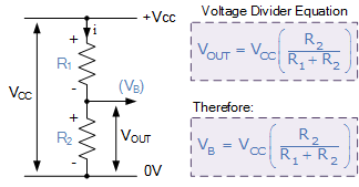
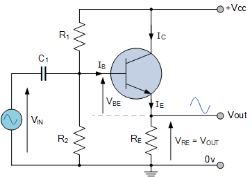 Resistors R1 and R2 form a simple voltage divider network used to bias the NPN transistor into conduction. Since this voltage divider lightly loads the transistor, the base voltage, VB can be easily calculated by using the simple voltage divider formula as shown.
Voltage Divider Network
With the collector terminal of the transistor connected directly to VCC and no collector resistance, (RC = 0) any collector current will generate a voltage drop across the emitter resistor RE.
However, in the common collector amplifier circuit, the same voltage drop, VE also represents the output voltage, VOUT.
Ideally we would want the DC voltage drop across RE to be equal to half the supply voltage, VCC to make the transistors quiescent output voltage sit somewhere in the middle of the characteristics curves allowing for a maximum unclipped output signal. Thus the choice of RE depends greatly on IB and the transistors current gain Beta, β.
As the base-emitter pn-junction is forward biased, base current flows through the junction to the emitter encouraging transistor action causing a much larger collector current, IC to flow. Thus the emitter current is a combination of base current and collector current as: IE = IB + IC. However, as the base current is extremely small compared to the collector current, the emitter current is therefore approximately equal to the collector current. Thus IE ≈ IC
- As with the common emitter (CE) amplifier configuration, the input signal is applied to the transistors base terminal, and as we said previously, the amplifiers output signal is taken from the emitter emitter terminal.
- However, as there is only one forward biased pn-junction between the transistors base and its emitter terminal, any input signal applied to the base passes directly through the junction to the emitter. Therefore the output signal present at the emitter is in-phase with the applied input signal at the base.
- As the amplifiers output signal is taken from across the emitter load this type of transistor configuration is also known as an Emitter Follower circuit as the emitter output “follows” or tracks any voltage changes to the base input signal, except that it remains about 0.7 volts (VBE) below the base voltage.
- Having said that, the emitters pn-junction effectively acts as a forward biased diode and for small AC input signals this emitter diode junction has a resistance given by: r′e = 25mV/Ie where the 25mV is the thermal voltage of the junction at room temperature (25oC) and Ie is the emitter current.
- So as the emitter current increases, the emitter resistance decreases by a proportional amount.
- The base current which flows through this internal base-emitter junction resistance also flows out and through the externally connected emitter resistor, RE.
- These two resistances are series connected thus acting as a potential divider network creating a voltage drop.
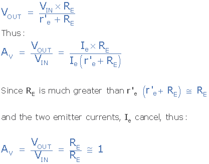
- Since the value of r′e is very small, and RE is much larger, usually in the kilohms (kΩ) range, the magnitude of the amplifiers output voltage is therefore less than its input voltage.
However, in reality the magnitude of the output voltage (peak-to-peak) is generally in the 98 to 99% value of the input voltage which is close enough in most cases to be considered as unity gain.
We can calculate the voltage gain, VA of the common collector amplifier by using the voltage divider formula as shown assuming that the base voltage, VB is actually the input voltage, VIN.
Common Collector Amplifier Voltage Gain
Common Collector Amplifier Example
A common collector amplifier is constructed using an NPN bipolar transistor and a voltage divider biasing network. If R1 = 5k6Ω, R2 = 6k8Ω and the supply voltage is 12 volts. Calculate the values of: VB, VC and VE, the emitter current IE, the internal emitter resistance r’e and the amplifiers voltage gain AV when a load resistance of 4k7Ω is used. Also draw the final circuit and corresponding characteristics curve with load line.
1. Base biasing voltage, VB

2. Collector voltage, VC. As there is no collector load resistance, the transistors collector terminal is connected directly to the DC supply rail, so VC = VCC = 12 volts.
3. Emitter biasing voltage, VE

4. Emitter Current, IE

5. AC Emitter Resistance, r’e

6. Voltage gain, AV

Common Collector Amplifier Circuit with Load Line
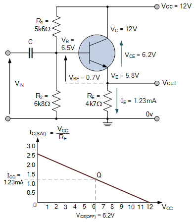
Common Collector Input Impedance
Although the common collector amplifier is not very good at being a voltage amplifier, because as we have seen, its small signal voltage gain is approximately equal to one (AV ≅ 1), it does however make a very good voltage buffer circuit due to its high input (ZIN) and low output (ZOUT) impedances, providing isolation between an input signal source from a load impedance load.
Another useful feature of the common collector amplifier is that it provides current gain (Ai) as long as it is conducting. That is it can pass a large current flowing from the collector to the emitter, in response to a small change to its base current, IB. Remember that this DC current only sees RE as there is no RC. Then the DC current is simply: VCC/RE which can be large if RE is small.
Consider the basic common collector amplifier or emitter follower configuration below:
Common Collector Amplifier Configuration
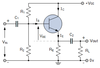
For AC analysis of the circuit, the capacitors are shorted and VCC is shorted (zero impedance). Thus the equivalent circuit is given as shown with the biasing currents and voltages given as:
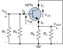
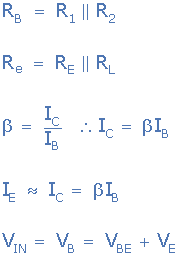
The Input Impedance, ZIN of the common collector configuration looking into the base is given as:
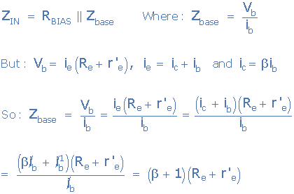
But as Beta, β is generally much greater than 1 (usually above 100), the expression of: β + 1 can be reduced to just Beta, β as multiplication by 100 is virtually the same as multiplying by 101. Thus:
Common Collector Amplifier Base Impedance

Where: β is the transistors current gain, Re is the equivalent emitter resistance, and r’e is the ac resistance of the emitter-base diode. Note that since the combined value of Re is generally much greater than the diodes equivalent resistance, r’e (kilo-ohms compared to a few ohms) the transistors base impedance can be given as simply: β*Re.
An interesting point to notice here is that the the transistors input base impedance, ZIN(base) can be controlled by the value of either the emitter leg resistor, RE or the load resistor RL as they are parallel connected.
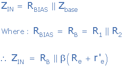
While the equation above gives us the input impedance looking into the base of the transistor, it does not give us the true input impedance that the source signal would see looking into the complete amplifier circuit. For that we need to consider the two resistors which make up the voltage divider biasing network. Thus:
Common Collector Amplifier Input Impedance
Collector Output Impedance
To determine the CC amplifiers output impedance ZOUT looking from the load back into the amplifiers emitter terminal, we must first remove the load as we want to see the effective resistance of the amplifier that is driving the load. Thus the AC equivalent circuit looking into the amplifiers output is given as:
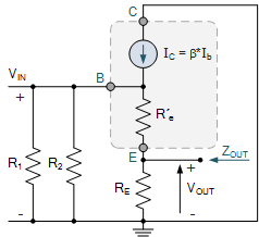
From above, the input impedance of the base circuit is given as:RB = R1||R2. The current gain of the transistor is given as: β. Thus the output equation is given as:

We can see then that the emitter resistor, RE is effectively in parallel with the whole impedance of the transistor looking back into its emitter terminal.
If we calculate the output impedance of our common emitter amplifier circuit using the component values from above, it would give an output impedance ZOUT of less than 50Ω (49.5Ω) which is much smaller than the higher input impedance, ZIN(BASE) calculated previously.
Thus we can see then that the Common Collector Amplifier configuration has, from calculation, a very high input impedance and a very low output impedance allowing it to drive a low impedance load. In fact due to the CC amplifiers relatively high input impedance and very low output impedance it is commonly used as a unity gain buffer amplifier.
Having determined that the output impedance, ZOUT of our example amplifier above is approximately 50Ω by calculation, if we now connect the 10kΩ load resistor back into the circuit, the resulting output impedance will be:

Although the load resistance is 10kΩ, the equivalent output resistance is still low at 49.3Ω. This is because RL is large compared with ZOUT, thus for maximum power transfer, RL must equal ZOUT. As the voltage gain of the common collector amplifier is considered to be unity (1), the amplifiers power gain must be equal to its current gain, as P = V*I.
Since the common collector current gain is defined as the ratio of the emitter current to the base current, γ = IE/IB = β + 1, it therefore follows that the amplifiers current gain must be approximately equal to Beta (β) as β + 1 is virtually the same as Beta.
Common Emitter Amplifier
To obtain low distortion when used as an amplifier the operating quiescent point needs to be correctly selected. This is in fact the DC operating point of the amplifier and its position may be established at any point along the load line by a suitable biasing arrangement.
The best possible position for this Q-point is as close to the center position of the load line as reasonably possible, thereby producing a Class A type amplifier operation, ie. Vce = 1/2Vcc. Consider the Common Emitter Amplifier circuit shown below.
The Common Emitter Amplifier Circuit
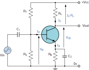
The single stage common emitter amplifier circuit shown above uses what is commonly called “Voltage Divider Biasing”. This type of biasing arrangement uses two resistors as a potential divider network across the supply with their center point supplying the required Base bias voltage to the transistor. Voltage divider biasing is commonly used in the design of bipolar transistor amplifier circuits.
 This method of biasing the transistor greatly reduces the effects of varying Beta, ( β ) by holding the Base bias at a constant steady voltage level allowing for best stability.
The quiescent Base voltage (Vb) is determined by the potential divider network formed by the two resistors, R1, R2 and the power supply voltage Vcc as shown with the current flowing through both resistors.
Then the total resistance RT will be equal to R1 + R2 giving the current as i = Vcc/RT. The voltage level generated at the junction of resistors R1 and R2 holds the Base voltage (Vb) constant at a value below the supply voltage.
The potential divider network used in the common emitter amplifier circuit divides the supply voltage in proportion to the resistance. This bias reference voltage can be easily calculated using the simple voltage divider formula below:
Transistor Bias Voltage

As the same supply voltage, (Vcc) also determines the maximum Collector current, Ic when the transistor is switched fully “ON” (saturation), Vce = 0. The Base current Ib for the transistor is found from the Collector current, Ic and the DC current gain Beta, β of the transistor.
Beta Value

A transistor’s Beta value, sometimes referred to as hFE on datasheets, defines the transistor’s forward current gain in the common emitter configuration. Beta is an electrical parameter built into the transistor during manufacture. Beta (hFE) has no units as it is a fixed ratio of the two currents, Ic and Ib so a small change in the Base current will cause a large change in the Collector current.
One final point about Beta. Transistors of the same type and part number will have large variations in their Beta value. For example, the BC107 NPN Bipolar transistor can have a DC current gain Beta value of between 110 and 450 (data sheet value).
That is, one BC107 device may have a Beta value of 110, while another one may have a Beta value of 450, but they are both sold as BC107 npn transistors. The reason for this is that the value of Beta ( β ) is an inherent characteristic of the transistor’s construction and not of its operation. As the Base/Emitter junction is forward-biased, the Emitter voltage, Ve will be one junction voltage drop different to the Base voltage. If the voltage across the Emitter resistor is known then the Emitter current, Ie can be easily calculated using Ohm’s Law. The Collector current, Ic can be approximated, since it is almost the same value as the Emitter current.
Common Emitter Amplifier Example
A common emitter amplifier circuit has a load resistance, RL of 1.2kΩ and a supply voltage of 12v. Calculate the maximum Collector current (Ic) flowing through the load resistor when the transistor is switched fully “ON” (saturation), assume Vce = 0.
Also find the value of the Emitter resistor, RE if it has a voltage drop of 1v across it. Calculate the values of all the other circuit resistors assuming a standard NPN silicon transistor.

This then establishes point “A” on the Collector current vertical axis of the characteristics curves and occurs when Vce = 0. When the transistor is switched fully “OFF”, there is no voltage drop across either resistor RE or RL as no current is flowing through them. Then the voltage drop across the transistor, Vce is equal to the supply voltage, Vcc. This establishes point “B” on the horizontal axis of the characteristics curves.
Generally, the quiescent Q-point of the amplifier is with zero input signal applied to the Base, so the Collector sits about half-way along the load line between zero volts and the supply voltage, (Vcc/2). Therefore, the Collector current at the Q-point of the amplifier will be given as:

This static DC load line produces a straight line equation whose slope is given as: -1/(RL + RE) and that it crosses the vertical Ic axis at a point equal to Vcc/(RL + RE). The actual position of the Q-point on the DC load line is determined by the mean value of Ib.
As the Collector current, Ic of the transistor is also equal to the DC gain of the transistor (Beta), times the Base current (β*Ib), if we assume a Beta (β) value for the transistor of say 100, (one hundred is a reasonable average value for low power signal transistor) the Base current Ib flowing into the transistor will be given as:

Instead of using a separate Base bias supply, it is usual to provide the Base Bias Voltage from the main supply rail (Vcc) through a dropping resistor, R1. Resistors, R1 and R2 can now be chosen to give a suitable quiescent Base current of 45.8μA or 46μA rounded off to the nearest integer. The current flowing through the potential divider circuit has to be large compared to the actual Base current, Ib, so that the voltage divider network is not loaded by the Base current flow.
A general rule of thumb is a value of at least 10 times Ib flowing through the resistor R2. Transistor Base/Emitter voltage, Vbe is fixed at 0.7V (silicon transistor) then this gives the value of R2 as:

If the current flowing through resistor R2 is 10 times the value of the Base current, then the current flowing through resistor R1 in the divider network must be 11 times the value of the Base current. That is: IR2 + Ib.
Thus the voltage across resistor R1 is equal to Vcc – 1.7v (VRE + 0.7 for silicon transistor) which is equal to 10.3V, therefore R1 can be calculated as:

The value of the Emitter resistor, RE can be easily calculated using Ohm’s Law. The current flowing through RE is a combination of the Base current, Ib and the Collector current Ic and is given as:

Resistor, RE is connected between the transistor’s Emitter terminal and ground, and we said previously that there is a voltage drop of 1 volt across it. Thus the value of the Emitter resistor, RE is calculated as:

So, for our example above, the preferred values of the resistors chosen to give a tolerance of 5% (E24) are:

Then, our original Common Emitter Amplifier circuit above can be rewritten to include the values of the components that we have just calculated above.
Question for Bipolar Junction Transistor AmplifiersTry yourself: What is the purpose of voltage divider biasing in a common emitter amplifier circuit?
View Solution
Completed Common Emitter Circuit

Amplifier Coupling Capacitors
In Common Emitter Amplifier circuits, capacitors C1 and C2 are used as Coupling Capacitors to separate the AC signals from the DC biasing voltage. This ensures that the bias condition set up for the circuit to operate correctly is not affected by any additional amplifier stages, as the capacitors will only pass AC signals and block any DC component. The output AC signal is then superimposed on the biasing of the following stages. Also a bypass capacitor, CE is included in the Emitter leg circuit.
This capacitor is effectively an open circuit component for DC biasing conditions, which means that the biasing currents and voltages are not affected by the addition of the capacitor maintaining a good Q-point stability.
However, this parallel connected bypass capacitor effectively becomes a short circuit to the Emitter resistor at high frequency signals due to its reactance. Thus only RL plus a very small internal resistance acts as its load increasing voltage gain to its maximum. Generally, the value of the bypass capacitor, CE is chosen to provide a reactance of at most, 1/10th the value of RE at the lowest operating signal frequency.
Output Characteristics Curves
Ok, so far so good. We can now construct a series of curves that show the Collector current, Ic against the Collector/Emitter voltage, Vce with different values of Base current, Ib for our simple common emitter amplifier circuit.
These curves are known as the “Output Characteristic Curves” and are used to show how the transistor will operate over its dynamic range. A static or DC load line is drawn onto the curves for the load resistor RL of 1.2kΩ to show all the transistor’s possible operating points.
When the transistor is switched “OFF”, Vce equals the supply voltage Vcc and this is point “B” on the line. Likewise, when the transistor is fully “ON” and saturated the Collector current is determined by the load resistor, RL and this is point “A” on the line.
We calculated before from the DC gain of the transistor that the Base current required for the mean position of the transistor was 45.8μA and this is marked as point Q on the load line which represents the Quiescent point or Q-point of the amplifier. We could quite easily make life easy for ourselves and round off this value to 50μA exactly, without any effect to the operating point.
Output Characteristics Curves

Point Q on the load line gives us the Base current Q-point of Ib = 45.8μA or 46μA. We need to find the maximum and minimum peak swings of Base current that will result in a proportional change to the Collector current, Ic without any distortion to the output signal.
As the load line cuts through the different Base current values on the DC characteristics curves we can find the peak swings of Base current that are equally spaced along the load line. These values are marked as points “N” and “M” on the line, giving a minimum and a maximum Base current of 20μA and 80μA respectively.
These points, “N” and “M” can be anywhere along the load line that we choose as long as they are equally spaced from Q. This then gives us a theoretical maximum input signal to the Base terminal of 60μA peak-to-peak, (30μA peak) without producing any distortion to the output signal.
Any input signal giving a Base current greater than this value will drive the transistor to go beyond point “N” and into its “cut-off” region or beyond point “M” and into its Saturation region thereby resulting in distortion to the output signal in the form of “clipping”.
Using points “N” and “M” as an example, the instantaneous values of Collector current and corresponding values of Collector-emitter voltage can be projected from the load line. It can be seen that the Collector-emitter voltage is in anti-phase (–180o) with the collector current.
As the Base current Ib changes in a positive direction from 50μA to 80μA, the Collector-emitter voltage, which is also the output voltage decreases from its steady state value of 5.8 volts to 2.0 volts.
Then a single stage Common Emitter Amplifier is also an “Inverting Amplifier” as an increase in Base voltage causes a decrease in Vout and a decrease in Base voltage produces an increase in Vout. In other words, the output signal is 180o out-of-phase with the input signal.
Common Emitter Voltage Gain
The Voltage Gain of the common emitter amplifier is equal to the ratio of the change in the input voltage to the change in the amplifier’s output voltage. Then ΔVL is Vout and ΔVB is Vin. But voltage gain is also equal to the ratio of the signal resistance in the Collector to the signal resistance in the Emitter and is given as:

We mentioned earlier that as the ac signal frequency increases the bypass capacitor, CE starts to short out the Emitter resistor due to its reactance. Then at high frequencies RE = 0, making the gain infinite.

However, the bipolar transistor has a small internal resistance built into its Emitter region called r’e. The transistor’s semiconductor material offers an internal resistance to the flow of current through it and is generally represented by a small resistor symbol shown inside the main transistor symbol.
Transistor data sheets tell us that for a small signal bipolar transistor this internal resistance is the product of 25mV ÷ Ie (25mV being the internal volt drop across the Emitter junction layer), then for our common Emitter amplifier circuit above this resistance value will be equal to:

This internal Emitter leg resistance will be in series with the external Emitter resistor, RE, then the equation for the transistor’s actual gain will be modified to include this internal resistance so will be:

At low frequency signals the total resistance in the Emitter leg is equal to RE + r’e. At high frequency, the bypass capacitor shorts out the Emitter resistor leaving only the internal resistance r’e in the Emitter leg resulting in a high gain.
Then for our common emitter amplifier circuit above, the gain of the circuit at both low and high signal frequencies is given as:
Amplifier Gain at Low Frequencies

Amplifier Gain at High Frequencies

|
137 videos|144 docs|71 tests
|


