Design of Amplifier: Examples - Electrical Engineering (EE) PDF Download

Design of Amplifier :
Example -1 (Common Emitter Amplifier Design)
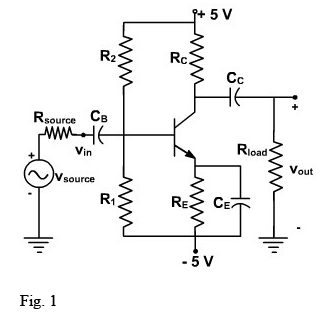
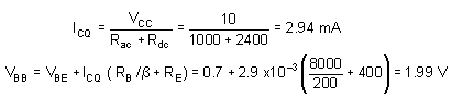
Design a common-emitter amplifier with a transistor having a β =200 and VBE = 0.7 V. Obtain an overall gain of |AV | ≥ 100 and maximum output voltage swing. Use the CE configuration shown in fig. 1 with two power supplies. Rsource is the resistance associated with the source, vsource. Let Rsource= 100 Ohms. The output load is 2KΩ. Determine the resistor values of the bias circuitry, the maximum undistorted output voltage swing, and the stage voltage gain.
Solution:
The maximum voltage across the amplifier is 10 V since the power supply can be visualized as a 10V power supply with a ground in the center. In this case, the ground has no significance to the operation of the amplifier since the input and output are isolated from the power supplies by capacitors.
We will have to select the value for RC and we are really not given enough information to do so.
Let us choose RC = Rload.
We don't have enough information to solve for RB – we can't use the bias stability criterion since we don't have the value of RE either. We will have to (arbitrarily) select a value of RB or RE. If this leads to a contradiction, or “bad” component values (e.g., unobtainable resistor values), we can come back and modify our choice. Let us select a value for RE that is large enough to obtain a reasonable value of VBB, Selecting RE as 400Ω will not appreciably reduce the collector current yet it will help in maintaining a reasonable value of VBB. Thus,
RB = 0.1 β RE = 0.1 (200)(400) = 8 K Ω
To insure that we have the maximum voltage swing at the output, we will use
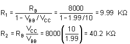
Note that we are carrying out our calculations to four places so that we can get accuracy to three places. The bias resistors are determined by-
Since we designed the bias circuit to place the quiescent point in the middle of the ac load line, we can use
Vout(undistorted p-p) 1.8 (2.94 x 10⁻³ ) (2 K Ω || 2 K Ω ) =5.29 V
Now we can determine the gain of the amplifier itself.
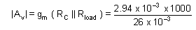
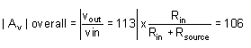
Using voltage division, we can determine the gain of the overall circuit.
The value of Rin can be obtained as
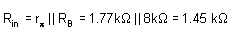
Thus the overall gain of the amplifier is
This shows that the common-emitter amplifier provides high voltage gain. However, it is very noisy, it has a low input impedance, and it does not have the stability of the emitter resistor common emitter amplifier.
Design of Amplifier
Example-2 (Emitter-Resistor Amplifier Design)
Design an emitter-resistor amplifier as shown in fig. 2 to drive a 2 KΩ load using a pnp silicon transistor, VCC = -24V, β = 200, Av = -10, and VBE = -0.7 V. Determine all element values and calculate Ai, Rin, ICQ and the maximum undistorted symmetrical output voltage swing for three values of RC as given below:
1. RC = Rload
2. RC = 0.1 Rload
3.RC = 10 Rload
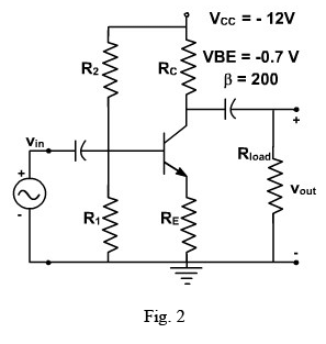
Solution:
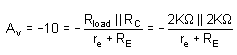
(a) RC = Rload
We use the various equations derived in previous lecture in order to derive the parameters of the circuit.
From the voltage gain, we can solve for R'E.
So r'E = re + RE = 100 Ω
We can find the quiescent value of the collector current IC from the collector-emitter loop using the equation for the condition of maximum output swing.
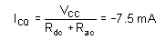
Therefore, 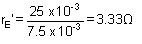
This is small enough that we shall ignore it to find that RE = 100 Ω. Since we now know β and RE.
We can use the design guideline.
RB = 0.1 β RE = 2 k Ω
As designed earlier, the biasing circuitry can be designed in the same manner and given by
VBB = -1.52 V
R1 = 2.14 K Ω
R2 = 3.6 K Ω
The maximum undistorted symmetrical peak to peak output swing is then
Vout (P-P) = 1.8 ICQ (Rload || RC ) = 13.5 V
Thus current gain Ai = -9.1
and input impedance Rin = 1.82 K Ω
(b) RC = 0.1 Rload
we repeat the steps of parts (a) to find
RC =200 Ω | Ri = 390 Ω |
ICQ =-57.4 mA | R2 =4.7K Ω |
r'e = 0.45 Ω | vout(p-p) = 18.7 V |
RB = 360 Ω | Ai = -1.64 |
VBB = -1.84 V | Rin = 327 Ω |
(C) RC =10 Rload
Once again, we follow the steps of part (a) to find
RC =20 K Ω | R1 =3.28K Ω |
ICQ =-1.07 mA | R2 = 85.6K Ω |
r'e = 24.2 Ω | vout(p-p) = 3.9 V |
RB = 3.64K Ω | Ai =-14.5 |
VBB = -0.886 V | Rin = 2.91K W |
We now compare the results obtained Table-I for the purpose of making the best choice for RC.
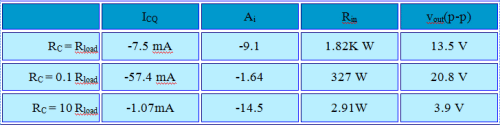
Table - 1 Comparsion for the three selections of RC
It indicates that of the three given ratios of RC to Rload, RC = Rload has the most desirable performance in the CE amplifier stage.
It can be used as a guide to develop reasonable designs. In most cases, this choice will provide performance that meets specifications. In some applications, it may be necessary to do additional analysis to find the optimum ratio of RC to Rload.
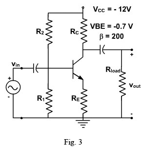
Design of Amplifier Example- 3 (Capacitor-Coupled Emitter-Resistor Amplifier Design) Design an emitter-resistor amplifier as shown in fig. 3 with AV =-10, β =200 and Rload = 1K Ω.
A pnp transistor is used and maximum symmetrical output swing is required.
Solution:
As designed earlier, we shall chose RC = Rload = 10 kΩ.
The voltage gain is given by 
where R'E= RE + r'e.
Substituting AV, Rload and RC in this equation, we find R'E= 50 Ω.
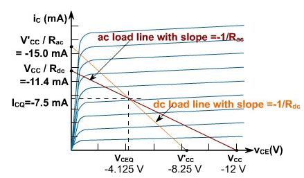
We need to know the value of r'e to find RE. We first find Rac and Rdc, and then calculate the Q point as follows (we assume r'e is small, so RE = R'E)
Rac = RE + RC || Rload = 550 Ω
Rdc = RE + RC = 1050 Ω
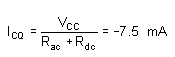
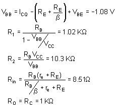
Now, the first step is to calculate the quiescent collector current needed to place the Q-point into the center of the ac load line (i.e., maximum swing). The equation is
The quantity, r'e , is found as follows
Then
RE = 50 - re = 46.67 Ω
If there were a current gain or input resistance specification for this design, we would use it to solve for the value of RB. Since is no such specification, we use the expression
RB =0.1 β RE = 0.1 (200) (46.6) = 932 Ω Then continuing with the design steps,
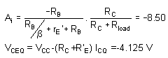
and
The last equality assumes that rO is large compared to RC.
The maximum undistorted peak to peak output swing is given by
1.8 | ICQ | ( RC || Rload )=1.8 ( 0.0075 ) ( 500 ) = 6.75 V
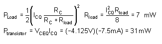
The power delivered into the load and the maximum power dissipated by the transistor are found as
The load lines for this circuit are shown in fig. 4.
FAQs on Design of Amplifier: Examples - Electrical Engineering (EE)
| 1. What is the purpose of an amplifier? |  |
| 2. What are the different types of amplifiers? | |
| 3. How does an amplifier work? | |
| 4. What are the key characteristics to consider when choosing an amplifier? | |
| 5. Can amplifiers be used for both audio and radio frequency signals? | |


mock tests for examination
,past year papers
,practice quizzes
,MCQs
,Sample Paper
,Extra Questions
,Semester Notes
,study material
,Viva Questions
,Summary
,ppt
,shortcuts and tricks
,Free
,Previous Year Questions with Solutions
,Important questions
,Exam
,Design of Amplifier: Examples - Electrical Engineering (EE)
,Objective type Questions
,Design of Amplifier: Examples - Electrical Engineering (EE)
,Design of Amplifier: Examples - Electrical Engineering (EE)
,video lectures
;


Design of Amplifier: Examples Free PDF Download
Importance of Design of Amplifier: Examples
Design of Amplifier: Examples Notes
Design of Amplifier: Examples Electrical Engineering (EE) Questions
Study Design of Amplifier: Examples on the App
|
© EduRev
|
Education Revolution
|


|


