Feedback and Oscillator Circuit (Part - 1) - Electrical Engineering (EE) PDF Download

Operational amplifier
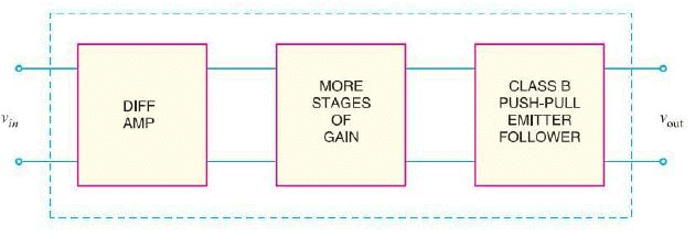
An operational amplifier(OP-Amp) is a circuit that can perform such mathematical operations as addition, subtraction, integration and differentiation. Fig.1 shows the block diagram of an operational amplifier. Note that OP-Amp is a multistage amplifier. The three stages are : differential amplifier input stage followed by a high-gain CEamplifier and finally the output stage.
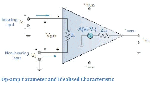
An Operational Amplifier is basically a three-terminal device which consists of two high impedance inputs, one called the Inverting Input, marked with a negative or “minus” sign, ( - ) and the other one called the Non-inverting Input, marked with a positive or “plus” sign ( + ).
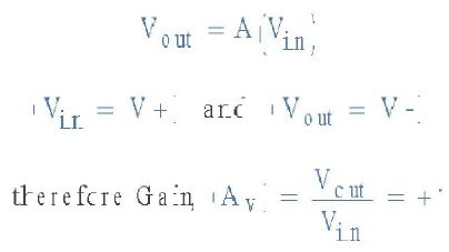
The third terminal represents the Operational Amplifiers output port which can both sink and source either a voltage or a current. In a linear operational amplifier, the output signal is the amplification factor, known as the amplifiers gain ( A ) multiplied by the value of the input signal and depending on the nature of these input and output signals, there can be four different classifications of operational amplifier gain.
Voltage – Voltage “in” and Voltage “out”
Current – Current “in” and Current “out”
Transconductance – Voltage “in” and Current “out”
Transresistance – Current “in” and Voltage “out”
Equivalent Circuit of an Ideal Operational Amplifier
Open Loop Gain, (Avo) Infinite – The main function of an operational amplifier is to amplify the input signal and the more open loop gain it has the better. Open-loop gain is the gain of the opamp without positive or negative feedback and for such an amplifier the gain will be infinite but typical real values range from about 20,000 to 200,000.
Input impedance, (Zin)
- Infinite – Input impedance is the ratio of input voltage to input current and is assumed to be infinite to prevent any current flowing from the source supply into the amplifiers input circuitry ( Iin = 0 ). Real op-amps have input leakage currents from a few pico-amps to a few milli-amps.
Output impedance, (Zout)
- Zero – The output impedance of the ideal operational amplifier is assumed to be zero acting as a perfect internal voltage source with no internal resistance so that it can supply as much current as necessary to the load. This internal resistance is effectively in series with the load thereby reducing the output voltage available to the load. Real op-amps have output impedances in the 100-20k range.
Bandwidth, (BW)
- Infinite – An ideal operational amplifier has an infinite frequency response and can amplify any frequency signal from DC to the highest AC frequencies so it is therefore assumed to have an infinite bandwidth. With real op-amps, the bandwidth is limited by the Gain-Bandwidth product (GB), which is equal to the frequency where the amplifiers gain becomes unity.
Offset Voltage, (Vio)
- Zero – The amplifiers output will be zero when the voltage difference between the inverting and the non-inverting inputs is zero, the same or when both inputs are grounded. Real op-amps have some amount of output offset voltage.
Open-loop Frequency Response Curve

From this frequency response curve we can see that the product of the gain against frequency is constant at any point along the curve. Also that the unity gain (0dB) frequency also determines the gain of the amplifier at any point along the curve. This constant is generally known as the Gain Bandwidth Product or GBP. Therefore:
GBP = Gain x Bandwidth or A x BW.
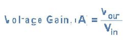
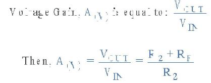
The Voltage Gain (AV) of the operational amplifier can be found using the following formula:
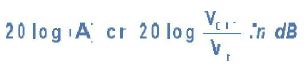
and in Decibels or (dB) is given as:
An Operational Amplifiers Bandwidth
The operational amplifiers bandwidth is the frequency range over which the voltage gain of the amplifier is above 70.7% or -3dB (where 0dB is the maximum) of its maximum output value as shown below.
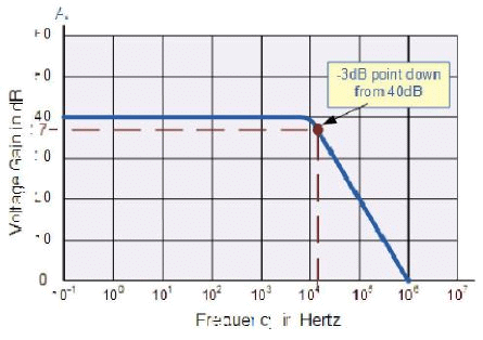
Here we have used the 40dB line as an example. The -3dB or 70.7% of Vmax down point from the frequency response curve is given as 37dB. Taking a line across until it intersects with the main GBP curve gives us a frequency point just above the 10kHz line at about 12 to 15kHz. We can now calculate this more accurately as we already know the GBP of the amplifier, in this particular case 1MHz.
Operational Amplifiers Summary
We know now that an Operational amplifiers is a very high gain DC differential amplifier that uses one or more external feedback networks to control its response and characteristics. We can connect external resistors or capacitors to the op-amp in a number of different ways to form basic “building Block” circuits such as, Inverting, Non-Inverting, Voltage Follower, Summing, Differential, Integrator and Differentiator type amplifiers.
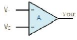
Op-amp Symbol
An “ideal” or perfect Operational Amplifier is a device with certain special characteristics such as infinite open-loop gain Ao, infinite input resistance Rin, zero output resistance Rout, infinite bandwidth 0 to and zero offset (the output is exactly zero when the input is zero).
There are a very large number of operational amplifier IC’s available to suit every possible application from standard bipolar, precision, high-speed, low-noise, highvoltage, etc, in either standard configuration or with internal Junction FET transistors.
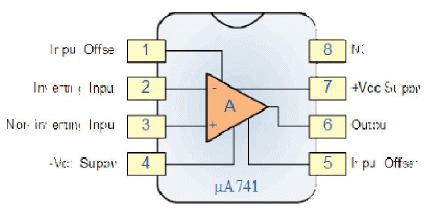
Operational amplifiers are available in IC packages of either single, dual or quad op-amps within one single device. The most commonly available and used of all operational amplifiers in basic electronic kits and projects is the industry standard A-741.
In the next tutorial about Operational Amplifiers, we will use negative feedback connected around the op-amp to produce a standard closed-loop amplifier circuit called an Inverting Amplifier circuit that produces an output signal which is 180 o “out-of-phase” with the input.
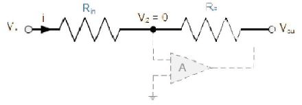
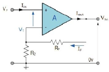
The Inverting Operational Amplifier
As the open loop DC gain of an Operational Amplifiers is extremely high we can therefore afford to lose some of this high gain by connecting a suitable resistor across the amplifier from the output terminal back to the inverting input terminal to both reduce and control the overall gain of the amplifier. This then produces and effect known commonly as Negative Feedback, and thus produces a very stable Operational Amplifier based system.
Negative Feedback is the process of “feeding back” a fraction of the output signal back to the input, but to make the feedback negative, we must feed it back to the negative or “inverting input” terminal of the op-amp using an external Feedback Resistor called Rƒ. This feedback connection between the output and the inverting input terminal forces the differential input voltage towards zero.
This effect produces a closed loop circuit to the amplifier resulting in the gain of the amplifier now being called its Closed-loop Gain. Then a closed-loop inverting amplifier uses negative feedback to accurately control the overall gain of the amplifier, but at a cost in the reduction of the amplifiers gain.
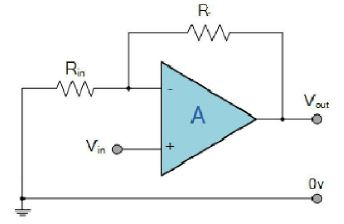
This negative feedback results in the inverting input terminal having a different signal on it than the actual input voltage as it will be the sum of the input voltage plus the negative feedback voltage giving it the label or term of a Summing Point. We must therefore separate the real input signal from the inverting input by using an Input Resistor, Rin.
As we are not using the positive non-inverting input this is connected to a common ground or zero voltage terminal as shown below, but the effect of this closed loop feedback circuit results in the voltage potential at the inverting input being equal to that at the non-inverting input producing a Virtual Earth summing point because it will be at the same potential as the grounded reference input. In other words, the op-amp becomes a “differential amplifier”.
Inverting Operational Amplifier Configuration
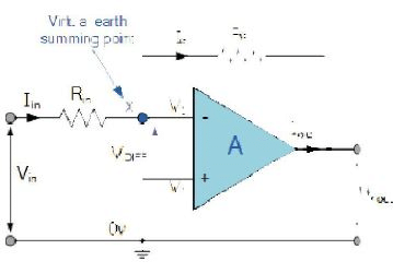
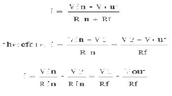
In this Inverting Amplifier circuit the operational amplifier is connected with feedback to produce a closed loop operation. When dealing with operational amplifiers there are two very important rules to remember about inverting amplifiers, these are: “No current flows into the input terminal” and that “V1 always equals V2”. However, in real world op-amp circuits both of these rules are slightly broken.
This is because the junction of the input and feedback signal ( X ) is at the same potential as the positive ( + ) input which is at zero volts or ground then, the junction is a “Virtual Earth”. Because of this virtual earth node the input resistance of the amplifier is equal to the value of the input resistor, Rin and the closed loop gain of the inverting amplifier can be set by the ratio of the two external resistors.
We said above that there are two very important rules to remember about Inverting Amplifiers or any operational amplifier for that matter and these are.
1. No Current Flows into the Input Terminals
2. The Differential Input Voltage is Zero as V1 = V2 = 0 (Virtual Earth)
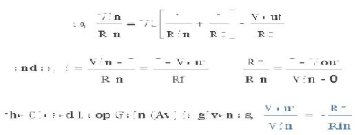
Then by using these two rules we can derive the equation for calculating the closedloop gain of an inverting amplifier, using first principles.
Current ( i ) flows through the resistor network as shown.
 .
.
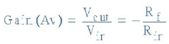
Then, the Closed-Loop Voltage Gain of an Inverting Amplifier is given as.
and this can be transposed to give Vout as:
The Non-inverting Operational Amplifier
Non-inverting Operational Amplifier Configuration
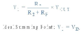
In the previous Inverting Amplifier tutorial, we said that for an ideal op-amp “No current flows into the input terminal” of the amplifier and that “V1 always equals V2”. This was because the junction of the input and feedback signal ( V1 ) are at the same potential.
In other words the junction is a “virtual earth” summing point. Because of this virtual earth node the resistors, Rƒ and R2 form a simple potential divider network across the non-inverting amplifier with the voltage gain of the circuit being determined by the ratios of R2 and Rƒ as shown below.
Equivalent Potential Divider Network
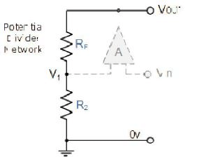
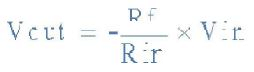
Then using the formula to calculate the output voltage of a potential divider network, we can calculate the closed-loop voltage gain ( A V ) of the Non-inverting Amplifier as follows:
 ..
..
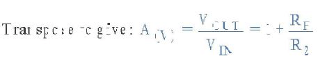
Then the closed loop voltage gain of a Non-inverting Operational Amplifier will be given as:
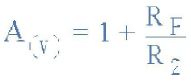
We can see from the equation above, that the overall closed-loop gain of a noninverting amplifier will always be greater but never less than one (unity), it is positive in nature and is determined by the ratio of the values of Rƒ and R2.
If the value of the feedback resistor Rƒ is zero, the gain of the amplifier will be exactly equal to one (unity). If resistor R2 is zero the gain will approach infinity, but in practice it will be limited to the operational amplifiers open-loop differential gain, ( Ao ).
We can easily convert an inverting operational amplifier configuration into a noninverting amplifier configuration by simply changing the input connections as shown.
Voltage Follower (Unity Gain Buffer)
If we made the feedback resistor, Rƒ equal to zero, (Rƒ = 0), and resistor R2 equal to infinity, (R2 = ), then the circuit would have a fixed gain of “1” as all the output voltage would be present on the inverting input terminal (negative feedback). This would then produce a special type of the non-inverting amplifier circuit called a Voltage Follower or also called a “unity gain buffer”.
As the input signal is connected directly to the non-inverting input of the amplifier the output signal is not inverted resulting in the output voltage being equal to the input voltage, Vout = Vin. This then makes the voltage follower circuit ideal as a Unity Gain Buffer circuit because of its isolation properties.
The advantage of the unity gain voltage follower is that it can be used when impedance matching or circuit isolation is more important than amplification as it maintains the signal voltage. The input impedance of the voltage follower circuit is very high, typically above 1M as it is equal to that of the operational amplifiers input resistance times its gain ( Rin x Ao ). Also its output impedance is very low since an ideal op-amp condition is assumed.
Non-inverting Voltage Follower
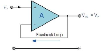
In this non-inverting circuit configuration, the input impedance Rin has increased to infinity and the feedback impedance Rƒ reduced to zero. The output is connected directly back to the negative inverting input so the feedback is 100% and Vin is exactly equal to Vout giving it a fixed gain of 1 or unity. As the input voltage Vin is applied to the non-inverting input the gain of the amplifier is given as:
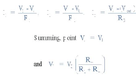
Differential Amplifier
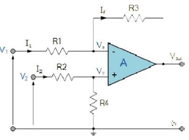
By connecting each input in turn to 0v ground we can use superposition to solve for the output voltage Vout. Then the transfer function for a Differential Amplifier circuit is given as:
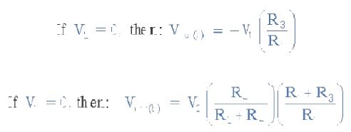
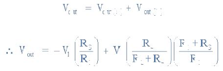
When resistors, R1 = R2 and R3 = R4 the above transfer function for the differential amplifier can be simplified to the following expression:
Differential Amplifier Equation
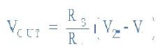
If all the resistors are all of the same ohmic value, that is: R1 = R2 = R3 = R4 then the circuit will become a Unity Gain Differential Amplifier and the voltage gain of the amplifier will be exactly one or unity. Then the output expression would simply be Vout = V2 - V1. Also note that if input V1 is higher than input V2 the output voltage sum will be negative, and if V2 is higher than V1, the output voltage sum will be positive.
The Differential Amplifier circuit is a very useful op-amp circuit and by adding more resistors in parallel with the input resistors R1 and R3, the resultant circuit can be made to either “Add” or “Subtract” the voltages applied to their respective inputs. One of the most common ways of doing this is to connect a “Resistive Bridge” commonly called a Wheatstone Bridge to the input of the amplifier as shown below.
Summing Amplifier Circuit
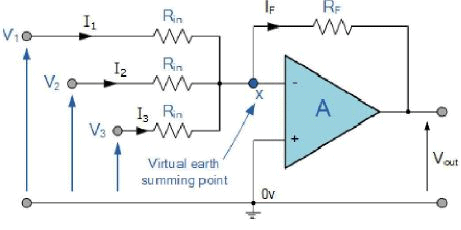
The output voltage, ( Vout ) now becomes proportional to the sum of the input voltages, V1, V2, V3 etc. Then we can modify the original equation for the inverting amplifier to take account of these new inputs thus:
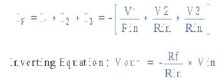
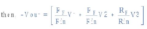
However, if all the input impedances, ( Rin ) are equal in value, we can simplify the above equation to give an output voltage of:
Summing Amplifier Equation
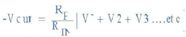
We now have an operational amplifier circuit that will amplify each individual input voltage and produce an output voltage signal that is proportional to the algebraic “SUM” of the three individual input voltages V1, V2 and V3. We can also add more inputs if required as each individual input “see’s” their respective resistance, Rin as the only input impedance.
This is because the input signals are effectively isolated from each other by the “virtual earth” node at the inverting input of the op-amp. A direct voltage addition can also be obtained when all the resistances are of equal value and Rƒ is equal to Rin.
Op-amp Differentiator Circuit
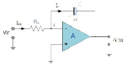
The input signal to the differentiator is applied to the capacitor. The capacitor blocks any DC content so there is no current flow to the amplifier summing point, X resulting in zero output voltage. The capacitor only allows AC type input voltage changes to pass through and whose frequency is dependant on the rate of change of the input signal.
At low frequencies the reactance of the capacitor is “High” resulting in a low gain ( Rƒ/Xc ) and low output voltage from the op-amp. At higher frequencies the reactance of the capacitor is much lower resulting in a higher gain and higher output voltage from the differentiator amplifier.
However, at high frequencies an op-amp differentiator circuit becomes unstable and will start to oscillate. This is due mainly to the first-order effect, which determines the frequency response of the op-amp circuit causing a second-order response which, at high frequencies gives an output voltage far higher than what would be expected. To avoid this the high frequency gain of the circuit needs to be reduced by adding an additional small value capacitor across the feedback resistor Rƒ.
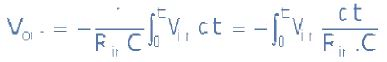
Ok, some math’s to explain what’s going on!. Since the node voltage of the operational amplifier at its inverting input terminal is zero, the current, i flowing through the capacitor will be given as:
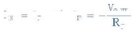
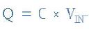
The charge on the capacitor equals Capacitance x Voltage across the capacitor
The rate of change of this charge is
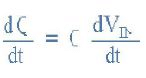
but dQ/dt is the capacitor current i
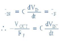
from which we have an ideal voltage output for the op-amp differentiator is given as:
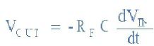
Therefore, the output voltage Vout is a constant -Rƒ.C times the derivative of the input voltage Vin with respect to time. The minus sign indicates a 180 o phase shift because the input signal is connected to the inverting input terminal of the operational amplifier.
One final point to mention, the Op-amp Differentiator circuit in its basic form has two main disadvantages compared to the previous Operational Amplifier Integrator circuit. One is that it suffers from instability at high frequencies as mentioned above, and the other is that the capacitive input makes it very susceptible to random noise signals and any noise or harmonics present in the source circuit will be amplified more than the input signal itself. This is because the output is proportional to the slope of the input voltage so some means of limiting the bandwidth in order to achieve closed-loop stability is required
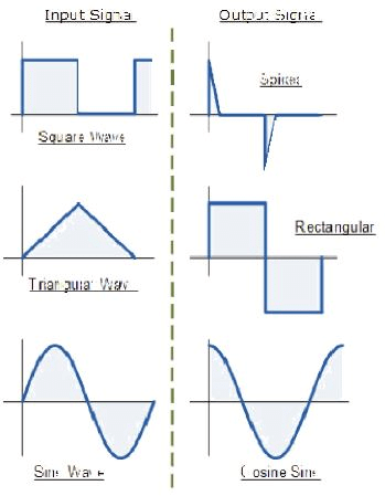
Op-amp Differentiator Waveforms
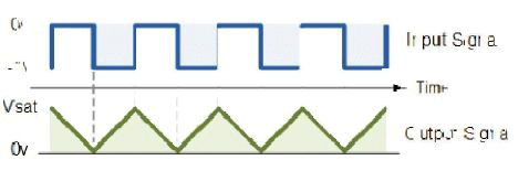
If we apply a constantly changing signal such as a Square-wave, Triangular or Sinewave type signal to the input of a differentiator amplifier circuit the resultant output signal will be changed and whose final shape is dependant upon the RC time constant of the Resistor/Capacitor combination.
Op-amp Integrator Circuit
As its name implies, the Op-amp Integrator is an Operational Amplifier circuit that performs the mathematical operation of Integration, that is we can cause the output to respond to changes in the input voltage over time as the op-amp integrator produces an output voltage which is proportional to the integral of the input voltage.
In other words the magnitude of the output signal is determined by the length of time a voltage is present at its input as the current through the feedback loop charges or discharges the capacitor as the required negative feedback occurs through the capacitor.
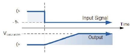
When a step voltage, Vin is firstly applied to the input of an integrating amplifier, the uncharged capacitor C has very little resistance and acts a bit like a short circuit allowing maximum current to flow via the input resistor, Rin as potential difference exists between the two plates. No current flows into the amplifiers input and point X is a virtual earth resulting in zero output. As the impedance of the capacitor at this point is very low, the gain ratio of Xc/Rin is also very small giving an overall voltage gain of less than one, ( voltage follower circuit ).
As the feedback capacitor, C begins to charge up due to the influence of the input voltage, its impedance Xc slowly increase in proportion to its rate of charge. The capacitor charges up at a rate determined by the RC time constant, ( ) of the series RC network. Negative feedback forces the op-amp to produce an output voltage that maintains a virtual earth at the op-amp’s inverting input.
Since the capacitor is connected between the op-amp’s inverting input (which is at earth potential) and the op-amp’s output (which is negative), the potential voltage, Vc developed across the capacitor slowly increases causing the charging current to decrease as the impedance of the capacitor increases. This results in the ratio of Xc/Rin increasing producing a linearly increasing ramp output voltage that continues to increase until the capacitor is fully charged.
At this point the capacitor acts as an open circuit, blocking any more flow of DC current. The ratio of feedback capacitor to input resistor ( Xc/Rin ) is now infinite resulting in infinite gain. The result of this high gain (similar to the op-amps open-loop gain), is that the output of the amplifier goes into saturation as shown below. (Saturation occurs when the output voltage of the amplifier swings heavily to one voltage supply rail or the other with little or no control in between).
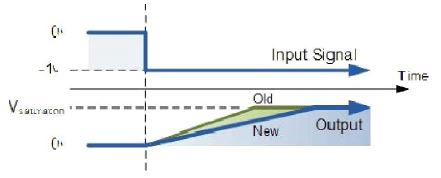
The rate at which the output voltage increases (the rate of change) is determined by the value of the resistor and the capacitor, “RC time constant“. By changing this RC time constant value, either by changing the value of the Capacitor, C or the Resistor, R, the time in which it takes the output voltage to reach saturation can also be changed for example.
If we apply a constantly changing input signal such as a square wave to the input of an Integrator Amplifier then the capacitor will charge and discharge in response to changes in the input signal. This results in the output signal being that of a sawtooth waveform whose frequency is dependant upon the RC time constant of the resistor/capacitor combination. This type of circuit is also known as a Ramp Generator and the transfer function is given below.
Op-amp Integrator Ramp Generator
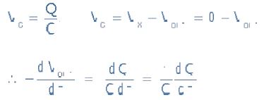
We know from first principals that the voltage on the plates of a capacitor is equal to the charge on the capacitor divided by its capacitance giving Q/C. Then the voltage across the capacitor is output Vout therefore: -Vout = Q/C. If the capacitor is charging and discharging, the rate of charge of voltage across the capacitor is given as:
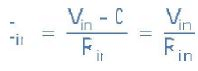
But dQ/dt is electric current and since the node voltage of the integrating op-amp at its inverting input terminal is zero, X = 0, the input current I(in) flowing through the input resistor, Rin is given as:
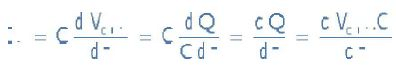
The current flowing through the feedback capacitor C is given as:
Assuming that the input impedance of the op-amp is infinite (ideal op-amp), no current flows into the op-amp terminal. Therefore, the nodal equation at the inverting input terminal is given as:
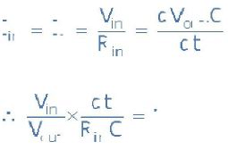
From which we derive an ideal voltage output for the Op-amp Integrator as:
To simplify the math’s a little, this can also be re-written as:
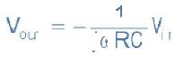
Where = 2 ƒ and the output voltage Vout is a constant 1/RC times the integral of the input voltage Vin with respect to time. The minus sign ( - ) indicates a 180o phase shift because the input signal is connected directly to the inverting input terminal of the op-amp.
FAQs on Feedback and Oscillator Circuit (Part - 1) - Electrical Engineering (EE)
| 1. What is feedback in an oscillator circuit? |  |
| 2. What is the role of an oscillator in an electronic circuit? | |
| 3. How does an oscillator circuit work? | |
| 4. What is the significance of frequency stability in an oscillator circuit? | |
| 5. What are the different types of oscillators used in electronic circuits? | |


Previous Year Questions with Solutions
,past year papers
,Free
,Feedback and Oscillator Circuit (Part - 1) - Electrical Engineering (EE)
,Semester Notes
,ppt
,Sample Paper
,Extra Questions
,Summary
,mock tests for examination
,study material
,shortcuts and tricks
,Objective type Questions
,Important questions
,Feedback and Oscillator Circuit (Part - 1) - Electrical Engineering (EE)
,video lectures
,Exam
,MCQs
,Viva Questions
,practice quizzes
,Feedback and Oscillator Circuit (Part - 1) - Electrical Engineering (EE)
;


Feedback and Oscillator Circuit (Part - 1) Free PDF Download
Importance of Feedback and Oscillator Circuit (Part - 1)
Feedback and Oscillator Circuit (Part - 1) Notes
Feedback and Oscillator Circuit (Part - 1) Electrical Engineering (EE) Questions
Study Feedback and Oscillator Circuit (Part - 1) on the App
|
© EduRev
|
Education Revolution
|


|


