Flip Flops | Analog and Digital Electronics - Electrical Engineering (EE) PDF Download
| Table of contents |

|
| Introduction |

|
| The RS Latch |

|
| SR Flip-flop ICs |

|
| Operation |

|
| The Data Latch |

|
| Ripple Through |

|
| Synchronous and Asynchronous Inputs |

|
| Timing Diagram |

|
Introduction
A circuit that has two stable states is treated as a flip flop. These stable states are used to store binary data that can be changed by applying varying inputs. The flip flops are the fundamental building blocks of the digital system. Flip flops and latches are examples of data storage elements. In the sequential logical circuit, the flip flop is the basic storage element. The latches and flip flops are the basic storage elements but different in working. There are the following types of flip flops:
SR Flip Flop
The S-R flip flop is the most common flip flop used in the digital system. In SR flip flop, when the set input "S" is true, the output Y will be high, and Y' will be low. It is required that the wiring of the circuit is maintained when the outputs are established. We maintain the wiring until set or reset input goes high, or power is shutdown.
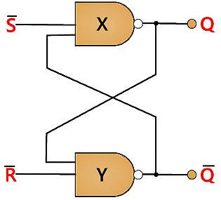
The S-R flip flop is the simplest and easiest circuit to understand.
Truth Table: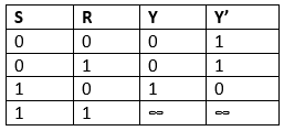
J-K Flip-flop
The JK flip flop is used to remove the drawback of the S-R flip flop, i.e., undefined states. The JK flip flop is formed by doing modification in the SR flip flop. The S-R flip flop is improved in order to construct the J-K flip flop. When S and R input is set to true, the SR flip flop gives an inaccurate result. But in the case of JK flip flop, it gives the correct output.
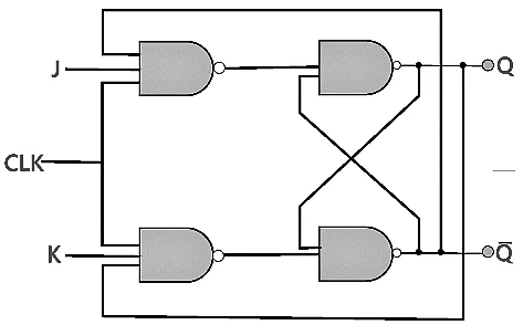
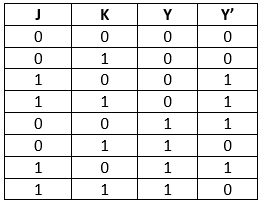
In J-K flip flop, if both of its inputs are different, the value of J at the next clock edge is taken by the output Y. If both of its input is low, then no change occurs, and if high at the clock edge, then from one state to the other, the output will be toggled. The JK Flip Flop is a Set or Reset Flip flop in the digital system.
Truth Table:
D Flip Flop
D flip flop is a widely used flip flop in digital systems. The D flip flop is mostly used in shift-registers, counters, and input synchronization.
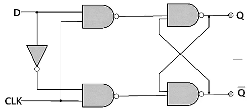
Truth Table: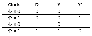
T Flip Flop
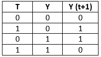
Just like JK flip-flop, T flip flop is used. Unlike JK flip flop, in T flip flop, there is only single input with the clock input. The T flip flop is constructed by connecting both of the inputs of JK flip flop together as a single input.
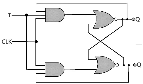
The T flip flop is also known as Toggle flip-flop. These T flip-flops are able to find the complement of its state.
Truth Table:
The RS Latch
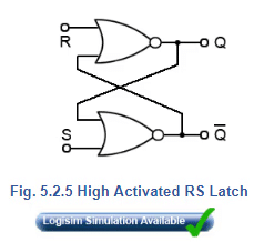
Flip-flops can also be considered as latch circuits due to them remembering or ‘latching’ a change at their inputs. A common form of RS latch is shown in Fig. 5.2.5. In this circuit the S and R inputs have now become inputs, meaning that they will now be ‘active high’.
They have also changed places, the R input is now on the gate having the Q output and the S input is on the gate. These changes occur because the circuit is using NOR gates instead of NAND.
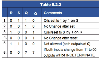
RS Latch Truth Table (Table 5.2.2)
- Q is set to 1 when the S input goes to logic 1.
- This is remembered on Q after the S input returns to logic 0.
- Q is reset set to 0 when the R input goes to logic 1.
- This is remembered on Q after the R input returns to logic 0.
- If both inputs are at logic 1, Q is the same as Q (the non-allowed state).
- The state of the outputs cannot be guaranteed if the inputs change from 1,1 to 0, 0 at the same time.
Timing Diagrams
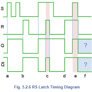
Truth tables are not always the best method for describing the action of a sequential circuit such as the SR flip-flop. Timing diagrams, which show how the logic states at various points in a circuit vary with time, are often preferred.
Fig. 5.2.6 shows a timing diagram describing the action of the basic RS Latch for logic changes at R and S. At time (a) S goes high and sets Q, which remains high until time (b) when S is low and R goes high, resetting Q. During period (c) both S and R are high causing the non-allowed state where both outputs are high. After period (c) Q remains high until time (d) when R goes high, resetting Q. Period (e) is another non-allowed period, at the end of which both inputs go low causing an indeterminate output condition in period (f).
The Clocked SR Flip-flop
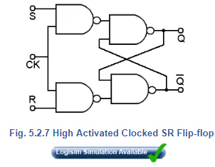
Fig. 5.2.7 shows a useful variation on the basic SR flip-flop, the clocked SR flip-flop. By adding two extra NAND gates, the timing of the output changeover after a change of logic states at S and R can be controlled by applying a logic 1 pulse to the clock (CK) input. Note that the inputs are now labelled S and R indicating that the inputs are now ‘high activated’. This is because the two extra NAND gates are disabled while the CK input is low, therefore the outputs are completely isolated from the inputs and so retain any previous logic state, but when the CK input is high (during a clock pulse) the input NAND gates act as inverters. Then for example, a logic 1 applied to S becomes a logic 0 applied to the S input of the active low SR flip-flop second stage circuit.
The main advantage of the CK input is that the output of this flip-flop can now be synchronised with many other circuits or devices that share the same clock. This arrangement could be used for a basic memory location by, for example, applying different logic states to a range of 8 flip-flops, and then applying a clock pulse to CK to cause the circuit to store a byte of data.
The basic form of the clocked SR flip-flop shown in Fig. 5.2.7 is an example of a level triggered flip-flop. This means that outputs can only change to a new state during the time that the clock pulse is at its high level (logic 1). The ability to change the input whilst CK is high can be a problem with this circuit, as any input changes occurring during the high CK period, will also change the outputs. A better method of triggering, which will only allow the outputs to change at one precise instant is provided by edge triggered devices available in D Type and JK flip-flops.
SR Flip-flop ICs
Comprising just two gates, low activated SR flip-flops are simple to implement using standard NAND gates but active low SR flip-flops (called SR flip-flops) are available as Quad packages in the LS TTL family as 74LS279 from Texas Instruments.
Circuit Symbols for Flip-flops
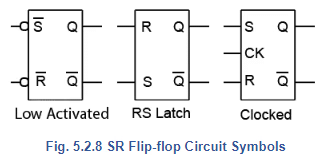
Rather than drawing the schematic circuit for individual gate versions of flip-flops it is common to draw them in block form. Some commonly used block versions of SR and RS flip-flops are shown in Fig. 5.2.8.
Typical applications for SR Flip-flops.
The basic building bock that makes computer memories possible, and is also used in many sequential logic circuits is the flip-flop or bi-stable circuit. Just two inter-connected logic gates make up the basic form of this circuit whose output has two stable output states. When the circuit is triggered into either one of these states by a suitable input pulse, it will ‘remember’ that state until it is changed by a further input pulse, or until power is removed. For this reason the circuit may also be called a Bi-stable Latch.
The SR flip-flop can be considered as a 1-bit memory, since it stores the input pulse even after it has passed. Flip-flops (or bi-stables) of different types can be made from logic gates and, as with other combinations of logic gates, the NAND and NOR gates are the most versatile, the NAND being most widely used. This is because, as well as being universal, i.e. it can be made to mimic any of the other standard logic functions, it is also cheaper to construct. Other, more widely used types of flip-flop are the JK, the D type and T type, which are developments of the SR flip-flop and will be studied in Modules 5.3 and 5.4.
The SR Flip-flop.
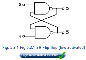
The SR (Set-Reset) flip-flop is one of the simplest sequential circuits and consists of two gates connected as shown in Fig. 5.2.1. Notice that the output of each gate is connected to one of the inputs of the other gate, giving a form of positive feedback or ‘cross-coupling’.
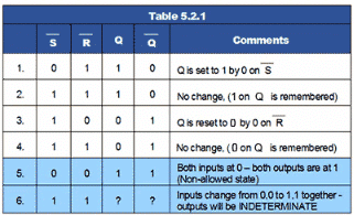
The circuit has two active low inputs marked S and R, ‘NOT’ being indicated by the bar above the letter, as well as two outputs, Q and Q. Table 5.2.1 shows what happens to the Q and Q outputs when a logic 0 is applied to either the S or R inputs.

The SR Flip-flop Truth Table (Table 5.2.1)
- Q output is set to logic 1 by applying logic 0 to the
input.
- Returning the S input to logic 1 has no effect. The 0 pulse (high-low-high) has been ‘remembered’ by the Q.
- Q is reset to 0 by logic 0 applied to the
input.
- As
returns to logic 1 the 0 on Q is ‘remembered’ by Q.
Problems with the SR Flip-flop
There are however, some problems with the operation of this most basic of flip-flop circuits. For conditions 1 to 4 in Table 5.2.1, is the inverse of Q. However, in row 5 both inputs are 0, which makes both Q and
= 1, and as they are no longer opposite logic states, although this state is possible, in practical circuits it is ‘not allowed’.
In row 6 both inputs are at logic 1 and the outputs are shown as ‘indeterminate’, this means that although Q and will be at opposite logic states it is not certain whether Q will be 1 or 0, Notice however that in the absence of any input pulses, both inputs are normally at logic 1. This is normally OK, as the outputs will be at the state remembered from the last input pulse. The indeterminate or uncertain logic state only occurs if the inputs change from 0,0 to 1,1 together. This should be avoided in normal operation, but is likely to happen when power is first applied. This could lead to uncertain results, but the flip-flop will work normally once an input pulse is applied to either input.
The SR Flip-flop is therefore, a simple 1-bit memory. If the S input is taken to logic 0 then back to logic 1, any further logic 0 pulses at will have no effect on the output.
D Type Flip-flops
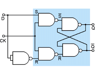
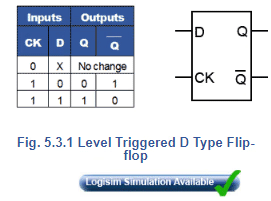
The major drawback of the SR flip-flop (i.e. its indeterminate output and non-allowed logic states) described in Digital Electronics Module 5.2 is overcome by the D type flip-flop. This flip-flop, shown in Fig. 5.3.1 together with its truth table and a typical schematic circuit symbol, may be called a Data flip-flop because of its ability to ‘latch’ and remember data, or a Delay flip-flop because latching and remembering data can be used to create a delay in the progress of that data through a circuit. To avoid the ambiguity in the title therefore, it is usually known simply as the D Type. The simplest form of D Type flip-flop is basically a high activated SR type with an additional inverter to ensure that the S and R inputs cannot both be high or both low at the same time. This simple modification prevents both the indeterminate and non-allowed states of the SR flip-flop. The S and R inputs are now replaced by a single D input, and all D type flip-flops have a clock input.
Operation
As long as the clock input is low, changes at the D input make no difference to the outputs. The truth table in Fig. 5.3.1 shows this as a ‘don’t care’ state (X). The basic D Type flip-flop shown in Fig. 5.3.1 is called a level triggered D Type flip-flop because whether the D input is active or not depends on the logic level of the clock input.
Provided that the CK input is high (at logic 1), then whichever logic state is at D will appear at output Q and (unlike the SR flip-flops) is always the inverse of Q).
In Fig. 5.3.1, if D = 1, then S must be 1 and R must be 0, therefore Q is SET to 1.
Alternatively,
If D = 0 then R must be 1 and S must be 0, causing Q to be reset to 0.
The Data Latch
The name Data Latch refers to a D Type flip-flop that is level triggered, as the data (1 or 0) appearing at D can be held or ‘latched’ at any time whilst the CK input is at a high level (logic 1).
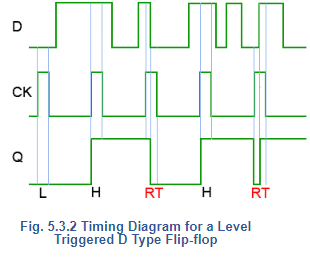
As can be seen from the timing diagram shown in Fig 5.3.2, if the data at D changes during this time, the Q output assumes the same logic level as the D.
Ripple Through
Fig. 5.3.2 also illustrates a possible problem with the level triggered D type flip-flop; if there are changes in the data during period when the clock pulse is at its high level, the logic state at Q changes in sympathy with D, and only ‘remembers’ the last input state that occurred during the clock pulse, (period RT in Fig. 5.3.2). This effect is called ‘Ripple Through’, and although this allows the level triggered D Type flip-flop to be used as a data switch, only allowing data through from D to Q as long as CK is held at logic 1, this may not be a desirable property in many types of circuit.
 The Edge Triggered D Type Flip-flop
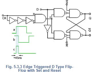
Fortunately ripple though can be largely prevented by using the Edge Triggered D Type flip-flop illustrated in Fig 5.3.3.
The clock pulse applied to the flip-flop is reduced to a very narrow positive going clock pulse of only about 45ns duration, by using an AND gate and applying the clock pulse directly to input ‘a’ but delaying its arrival at input ‘b’ by passing it through 3 inverters. This inverts the pulse and also delays it by three propagation delays, (about 15ns per inverter gate for 74HC series gates). The AND gate therefore produces logic 1 at its output only for the 45ns when both ‘a’ and ‘b’ are at logic 1 after the rising edge of the clock pulse.
Synchronous and Asynchronous Inputs
A further refinement in Fig. 5.3.3 is the addition of two further inputs SET and RESET, which are actually the original S and Rinputs of the basic low activated SR flip-flop.
Notice that there is now a subtle difference between the active low Set and Reset
inputs, and the D input. The D input is SYNCHRONOUS, that is its action is synchronised with the clock, but the
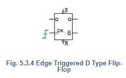
inputs are ASYNCHRONOUS i.e. their action is NOT synchronised with the clock. The SET and RESET inputs in Fig 5.3.4 are ‘low activated’, which is shown by the inversion circles at the S and R inputs to indicate that they are really
.
The flip-flop is positive edge triggered, which is shown on the CK input in Fig 5.3.4 by the wedge symbol. A wedge accompanied by an inversion circle would indicate negative (falling) edge triggering, though this is generally not used on D Type flip-flops.
Timing Diagram
The ‘Edge triggered D type flip-flop with asynchronous preset and clear capability’, although developed from the basic SR flip-flop becomes a very versatile flip-flop with many uses. A timing diagram illustrating the action of a positive edge triggered device is shown in Fig. 5.3.5.
At the positive going edges of clock pulses a and b, the D input is high so Q is also high.
Just before pulse c the D input goes low, so at the positive going edge of pulse c, Q goes low.
Between pulses c and d the asynchronous input goes low and immediately sets Q high.
The flip-flop then ignores pulse d while is low, but as
returns high, and D has also returned to its high state before pulse e, Q remains high during pulse e.
At the positive going edge of pulse h, the low level of input D remains, keeping Q low, but between pulses h and i, the S input goes low, overriding any action of D and immediately making Q high.
D is still high at the positive going edge of pulse f, and because the flip-flop is positive edge triggered, the change in the logic level of D during pulse f is ignored until the positive going edge of pulse g, which resets Q to its low level.
Clock pulse i is again ignored, due to being in its active low state and Q remains high, under the control of
until just before pulse j. At the positive going edge of pulse j, input D regains control, but as D is high and Q is already high, no change in output Q occurs.
Finally, just before pulse k, the asynchronous reset input goes low and resets Q to its low level (logic 0), which again causes the D input to be ignored.
|
135 videos|167 docs|71 tests
|
FAQs on Flip Flops - Analog and Digital Electronics - Electrical Engineering (EE)
| 1. What is the truth table for the RS Latch? |  |
| 2. What are some typical applications for SR Flip-flops? |  |
| 3. What are some problems with the SR Flip-flop? |  |
| 4. What is the difference between an RS Latch and an SR Flip-flop? |  |
| 5. How are flip-flops represented in circuit symbols? |  |


