Homojunction Devices - Semiconductor Devices, CSIR-NET Physical Sciences | Physics for IIT JAM, UGC - NET, CSIR NET PDF Download

A homojunction is a semiconductor interface that occurs between layers of similar semiconductor material, these materials have equal band gaps but typically have different doping. In most practical cases a homojunction occurs at the interface between an n-type (donor doped) and p-type (acceptor doped) semiconductor such as silicon, this is called a p-n junction.
This is not a necessary condition as the only requirement is that the same semiconductor (same band gap) is found on both sides of the junction, in contrast to a heterojunction. An n-type to n-type junction, for example, would be considered a homojunction if the doping levels are different.
The different doping level will cause band bending, and depletion region will be formed at the interface, as shown in the right figure.
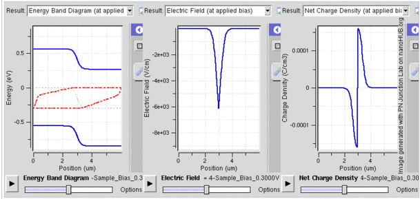
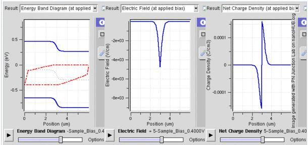
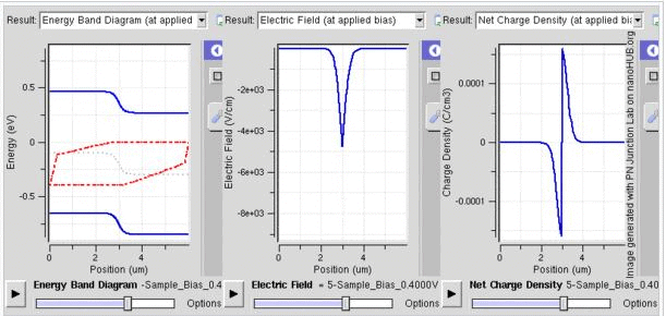
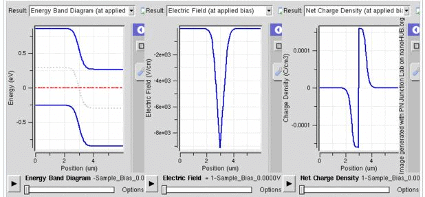
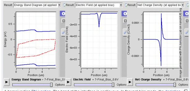
A homojunction PN junction. The band at the interface is continuous. In forward bias mode, the depletion width decreases. Both p and n junctions are doped at a 1e15/cm3 doping level, leading to built-in potential of ~0.59V. Observe the different Quasi Fermi levels for conduction band and valence band in n and p regions (red curves).
FAQs on Homojunction Devices - Semiconductor Devices, CSIR-NET Physical Sciences - Physics for IIT JAM, UGC - NET, CSIR NET
| 1. What are homojunction devices? |  |
| 2. How do homojunction devices work? | |
| 3. What are some examples of homojunction devices? | |
| 4. What are the advantages of homojunction devices? | |
| 5. What are the limitations of homojunction devices? | |


Previous Year Questions with Solutions
,MCQs
,study material
,CSIR-NET Physical Sciences | Physics for IIT JAM
,Homojunction Devices - Semiconductor Devices
,Homojunction Devices - Semiconductor Devices
,CSIR NET
,mock tests for examination
,Summary
,Semester Notes
,UGC - NET
,CSIR NET
,past year papers
,Important questions
,Extra Questions
,Exam
,Viva Questions
,practice quizzes
,UGC - NET
,shortcuts and tricks
,CSIR-NET Physical Sciences | Physics for IIT JAM
,Free
,CSIR NET
,ppt
,video lectures
,UGC - NET
,Objective type Questions
,Homojunction Devices - Semiconductor Devices
,CSIR-NET Physical Sciences | Physics for IIT JAM
,Sample Paper
;


Homojunction Devices - Semiconductor Devices, CSIR-NET Physical Sciences Free PDF Download
Importance of Homojunction Devices - Semiconductor Devices, CSIR-NET Physical Sciences
Homojunction Devices - Semiconductor Devices, CSIR-NET Physical Sciences Notes
Homojunction Devices - Semiconductor Devices, CSIR-NET Physical Sciences Physics Questions
Study Homojunction Devices - Semiconductor Devices, CSIR-NET Physical Sciences on the App
|
© EduRev
|
Education Revolution
|


|


