Irodov Solutions: Molecules and Crystals- 3 | I. E. Irodov Solutions for Physics Class 11 & Class 12 - JEE PDF Download
Q.201. Calculate the interval (in eV units) between neighbouring levels of free electrons in a metal at T = 0 near the Fermi level, if the concentration of free electrons is n = 2.0.1022 cm-3 and the volume of the metal is V = 1.0 cm3
Ans. We write the expression for the number of electrons as

Hence if A £ is the spacing between neighbouring levels near the Fermi level we must have

(2 on the RHS is to take care of both spins / electrons). Thus

But 
So
Substituting the data we get

Q.202. Making use of Eq. (6.4g), find at T = 0:
(a) the velocity distribution of free electrons;
(b) the ratio of the mean velocity of free electrons to their maximum velocity.
Ans. (a) From

we get on using 


This holds for 0 < v < vF where 
and 
(b) Mean velocity is


Q.203. On the basis of Eq. (6.4g) find the number of free electrons in a metal at T = 0 as a function of de Broglie wavelengths
Ans. Using the formula of the previous section

We put  where λ = de Broglie wavelength

Taking account of the fact that λ decreases when v increases we write

Q.204. Calculate the electronic gas pressure in metallic sodium, at T = 0, in which the concentration of free electrons is n = = 2.5.1022 cm-3. Use the equation for the pressure of ideal gas.
Ans. From the kinetic theory of gasses we know

Here U is the total interval energy of the gas. This result is applicable to Fermi gas also Now at T = 0

so 


Substituting the values we get
p = 4.92 x 10⁴ atmos
Q.205. The increase in temperature of a cathode in electronic tube by ΔT = 1.0 K from the value T= 2000 K results in the increase of saturation current by η = 1.4%. Find the work function of electron for the material of the cathode.
Ans. From Richardson's equation

where A is the work function in eV. When T increases by ΔT , I increases to (1 + η)I. Then


Expanding and neglecting higher powers of  we get

Thus 
Substituting we get A = 4.48 eV
Q.206. Find the refractive index of metallic sodium for electrons with kinetic energy T = 135 eV. Only one free electron is assumed to correspond to each sodium atom.
Ans.


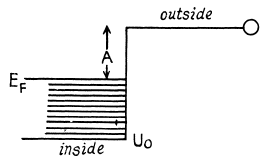
The potential energy inside the metal is - U0 for the electron and it related to the work function A by
U0 = Ep + A
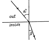
If T is the K.E. of electrons outside the metal, its K.E. inside the metal will be (E + U0) . On entering the metal electron connot experience any tangential force so the tangential component of momentum is unchanged. Then

Hence
 n by the definition of refractive index
In sodium with one free electron per Na atom
n = 2.54 x 10²² per c.c.
EF = 3.15 eV
A = 2.27 eV (from table)
U0 = 5.42 eV
n = 102
Q.207. Find the minimum energy of electron-hole pair formation in an impurity-free semiconductor whose electric conductance increases η = 5.0 times when the temperature increases from T1 = = 300 K to T2 = 400 K.
Ans. In a pure (intrinsic) semiconductor the conductivity is related to the temperature by the following formula very closely :

where Δε is the eneigy gap between the top of valence band and the bottom of conduction band; it is also the minimum energy required for the formation of electron-hole pair. The conductivity increases with temperature and we have

or 
Hence 
Substitution gives

Q.208. At very low temperatures the photoelectric threshold short wavelength in an impurity-free germanium is equal to λih = 1.7μm. Find the temperature coefficient of resistance of this germanium sample at room temperature.
Ans. The photoelectric threshold determines the band gap Δε by

On the other hand the temperature coefficient of resistance is defined by (p is resistivity)

where σ is the conductivity. But

Then 
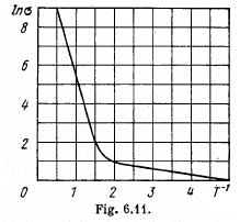
Q.209. Fig. 6.11 illustrates logarithmic electric conductance as a function of reciprocal temperature (7' in kK units) for some

n-type semiconductor. Using this plot, find the width of the forbidden band of the semiconductor and the activation energy of donor levels.
Ans. At high temperatures (small values of T-1) most of the conductivity is intrinsic i.e. it is due to the transition of electrons from the upper levels of the valance band into the lower levels of conduction vands.
For this we can apply approximately the formula

or 
From this we get the band gap

The slope must be calculated at small  Evaluation gives
  = 7000 K
Hence Eg = 1.21 eV
At low temperatures (high values of  ) the conductance is mostly due to impurities. If E0 is the ionization energy of donor levels then we can write the approximate formula (valid at low temperature)

So 
The slope must be calculated at low temperatures. Evaluation gives the slope

Then 
Q.210. The resistivity of an impurity-free semiconductor at room temperature is ρ = 50 Ω•cm. It becomes equal to ρi = 40 Ω•cm when the semiconductor is illuminated with light, and t = 8 ms after switching off the light source the resistivity becomes equal to ρ2 = 45 Ω•cm. Find the mean lifetime of conduction electrons and holes.
Ans. We write the conductivity of the sample as

where σi = intrinsic conductivity and σγ is the photo conductivity. At t = 0, assuming saturation we have


Time t after light source is switched off
we have because of recombination of electron and holes in the sample

where T = mean lifetime of electrons and holes.
Thus 
or 
or 
Hence 
Substitution gives 
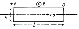
Q.211. In Hall effect measurements a plate of width h = 10 mm and length l = 50 mm made of p-type semiconductor was placed in a magnetic field with induction B = 5.0 kG. A potential difference V = 10 V was applied across the edges of the plate. In this case the Hall field is VH = 50 mV and resistivity ρ = 2.5 Ω•cm. Find the concentration of holes and hole mobility.
Ans.

We shall ignore minority carriers.
Drifting holes experience a sideways force in the magnetic field and react by setting up a Hall electric field Eγ to counterbalance it Thus

If the concentration of carriers is n then

Hence 
Also using 
we get 
Substituting the data (note that in MKS units B = 5.0 k G = 0.5 T)
ρ = 2.5 x 10⁻² ohm-m
we get n = 4.99 x 10²¹ m -3
= 4.99 x 10¹⁵ per cm3
Also the mobility is 
Substitution gives Uo = 0.05 m2/ V - s
Q.212. In Hall effect measurements in a magnetic field with induction B = 5.0 kG the transverse electric field strength in an impurity-free germanium turned out to be η = 10 times less than the longitudinal electric field strength. Find the difference in the mobilities of conduction electrons and holes in the given semiconductor.
Ans.

If an electric Geld Ex is present in a sample containing equal amounts of both electrons and holes, the two drift in opposite directions.
In the presence of a magnetic field Bz = B they set up Hall voltages in opposite directions.
The net Hall electric field is given by

But 

Substitution gives 
Q.213. The Hall effect turned out to be not observable in a semiconductor whose conduction electron mobility was η = 2.0 times that of the hole mobility. Find the ratio of hole and conduction electron concentrations in that semiconductor
Ans.

When the sample contains unequal number of carriers of both types whose mobilities are different, static equilibrium (i.e. no transverse movement of either electron or holes) is impossible in a magnetic Geld. The transverse electric Geld acts differently on electrons and holes. If the Ey that is set up is as shown, the net Lorentz force per unit charge (effective transverse electric Geld) on electrons is

and on holes

(we are assuming B = Bz). There is then a transverse drift of electrons and holes and the net transverse current must vanish in equilibrium. Using mobility

or 
On the other hand

Thus, the Hall coefficient is

We see that RH = 0 when


|
Explore Courses for JEE exam
|

|


