JEE Advanced (Single Correct Type): Semiconductor Electronics & Communication Systems | Chapter-wise Tests for JEE Main & Advanced PDF Download
Q.1. The typical ionisation energy of a donor in silicon is
(a) 10.0 eV
(b) 1.0 eV
(c) 0.1 eV
(d) 0.001 eV
Correct Answer is option (c)
When donor impurity (+5 valence) added to a pure silicon (+4 valence), the +5 donor atom sits in the place of +4 valence silicon atom. so it has a net additional +1 electronic charge. The four valence electron form covalent bond and get fixed in the lattice. The fifth electron (with net –1 electronic charge) can be approximated to revolve around +1 additional charge. The situation is like the hydrogen atom for which energy is given by. For the case of hydrogen, the permittivity was taken as ε0. However, if the medium has a permittivity εr , relative to ε0 , then
.
For Si, εr = 12 and for n ¾ 1, E = 0.1 eV
Q.2. In the circuit given below, V(t) is the sinusoidal voltage source, voltage drop VAB(t) across the resistance R is
(a) Is half wave rectified
(b) Is full wave rectified
(c) Has the same peak value in the positive and negative half cycles
(d) Has different peak values during positive and negative half cycle
Correct Answer is option (d)
In positive half cycle one diode is in forward biasing and other is in reverse biasing while in negative half cycle their polarity reverses, and direction of current is opposite through R for positive and negative half cycles so out put is not rectified. Since R1 and R2 are different hence the peaks during positive half and negative half of the input signal will be different.
Q.3. In the following circuits PN-junction diodes D1, D2 and D3 are ideal for the following potential of A and B, the correct increasing order of resistance between A and B will be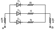 (i) – 10 V, –5 V
(ii) –5 V, – 10 V
(iii) – 4 V, –12 V
(a) (i) < (ii) < (iii)
(b) (iii) < (ii) < (i)
(c) (ii) ¾ (iiii) < (i)
(d) (i) ¾ (iii) < (ii)
Correct Answer is option (c)
(i) VA = -10 V and VB = -5 V Diodes D1 and D3 are reveres biased and D2 is forward biased.
⇒(ii) When VA = -5V and VB = -10 V Diodes D2 is reverse biased D1 and D3 are forward biased
⇒
(iii) In this case equivalent resistance between A and B is also R.Hence (ii) ¾ (iii) < (i).
Q.4. A piece of copper and the other of germanium are cooled from the room temperature to 80 K, then which of the following would be a correct statement
(a) Resistance of each increase
(b) Resistance of each decrease
(c) Resistance of copper increases while that of germanium decrease
(d) Resistance of copper decrease while that of germanium increase
Correct Answer is option (d)
Resistance of conductors (Cu) decreases with decrease in temperature while that of semiconductors (Ge) increases with decrease in temperature.
Q.5. Given below are symbols for some logic gates The XOR gate and NOR gate respectively are  (a) 1 and 2
(b) 2 and 3
(c) 3 and 4
(d) 1 and 4
Correct Answer is option (b)
Q.6. Which of the following gates will have an output of 1
(a) 
(b) 
(c) 
(d) 
Correct Answer is option (c)
For 'NAND' gate (option c), output =
Q.7. This symbol represents (a) NOT gate
(b) OR gate
(c) AND gate
(d) NOR gate
Correct Answer is option (a)
- NOT Gate
Q.8. Which logic gate is represented by the following combination of logic gates? (a) OR
(b) NAND
(c) AND
(d) NOR
Correct Answer is Option (c)
According to De Morgan's theorem
This is output equation of 'AND' gate.
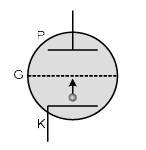
Q.9. For a given plate-voltage, the plate current in a triode is maximum when the potential of
(a) The grid is positive and plate is negative
(b) The grid is positive and plate is positive
(c) The grid is zero and plate is positive
(d) The grid is negative and plate is positive
Correct Answer is option (b)
When grid is given positive potential more electrons will cross the grid to reach the positive plate P. Hence current increases.
Q.10. A silicon specimen is made into a P-type semiconductor by doping, on an average, one Indium atom per 5 x 10⁷ silicon atoms. If the number density of atoms in the silicon specimen is 5 x 1028 atoms / m3 then the number of acceptor atoms in silicon per cubic centimetre will be
(a) 2.5 x 1030 atoms / cm3
(b) 1.0 x 10¹³ atoms / cm3
(c) 1.0 x 10¹⁵ atoms / cm3
(d) 2.5 x 1036 atoms / cm3
Correct Answer is option (c)
Number density of atoms in silicon specimen = 5 x 1028 atom/m3 = 5 x 10²² atom/cm3 Since one atom of indium is doped in =5 x 10⁷ Si atom. So number of indium atoms doped per cm3 of siliconatom/cm3.
Q.11. The probability of electrons to be found in the conduction band of an intrinsic semiconductor at a finite temperature
(a) Decreases exponentially with increasing band gap
(b) Increases exponentially with increasing band gap
(c) Decreases with increasing temperature
(d) Is independent of the temperature and the band gap
Correct Answer is option (a)
The probability of electrons to be found in the conduction band of an intrinsic semiconductorwhere k = Boltzman's constant.
Hence, at a finite temperature, the probability decreases exponentially with increasing band gap.
Q.12. A transistor is used as an amplifier in CB mode with a load resistance of 5 kW the current gain of amplifier is 0.98 and the input resistance is 70 W, the voltage gain and power gain respectively are
(a) 70, 68.6
(b) 80, 75.6
(c) 60, 66.6
(d) 90, 96.6
Correct Answer is option (a)
In common base mode α = 0.98 , R = 5 kΩ , Rin ¾ 70Ω
∴ voltage gain
Power gain ¾ Current gain x Voltage gain=0.98 x 70 = 68.6
Q.13. The circuit shown in following figure contains two diode D1 and D2 each with a forward resistance of 50 ohms and with infinite backward resistance. If the battery voltage is 6 V, the current through the 100 ohm resistance (in amperes) is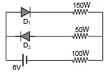 (a) Zero
(b) 0.02
(c) 0.03
(d) 0.036
Correct Answer is option (b)
According to the given polarity, diode D1 is forward biased while D2 is reverse biased. Hence current will pass through D1 only.
So, current
Q.14. In the circuit, if the forward voltage drop for the diode is 0.5 V, the current will be (a) 3.4 mA
(b) 2 mA
(c) 2.5 mA
(d) 3 mA
Correct Answer is option (a)
The voltage drop across resistance ¾ 8 – 0.5 ¾ 7.5 V
∴ Current= 3.4 mA
Q.15. The diode used in the circuit shown in the figure has a constant voltage drop of 0.5 V at all currents and a maximum power rating of 100 milliwatts. What should be the value of the resistor R, connected in series with the diode for obtaining maximum current?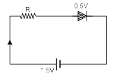 (a) 1.5 W
(b) 5 W
(c) 6.67 W
(d) 200 W
Correct Answer is option (b)
The current through circuit= 0.2 A
∴ voltage drop across resistance = 1.5 - 0.5 = 1 V
⇒
Q.16. The junction diode in the following circuit requires a minimum current of 1 mA to be above the knee point (0.7 V) of its I-V characteristics curve. Te voltage across the diode is independent of current above the knee point. If VB ¾ 5 V, then the maximum value of R so that the voltage is above the knee point, will be (a) 4.3 kΩ
(b) 860 kΩ
(c) 4.3 Ω
(d) 860 Ω
Correct Answer is option (a)
At knee point voltage across the diode is 0.7 V.
Hence voltage across resistance R is 5 - 0.7 = 4.3 V
⇒ using V = iR ⇒ 4.3 = 1 x 10⁻³ x R ⇒ R = 4.3 kΩ
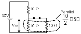
Q.17. Find VAB (a) 10 V
(b) 20 V
(c) 30 V
(d) None of these
Correct Answer is option (a)
Diode is in forwards biasing hence the circuit can be redrawn as follows
Q.18. The combination of the gates shown in the figure below produces (a) NOR gate
(b) OR gate
(c) AND gate
(d) XOR gate
Correct Answer is option (b)
This output equation is equivalent to OR gate.
Q.19. The output of OR gate is 1
(a) If both inputs are zero
(b) If either or both inputs are 1
(c) Only if both input are 1
(d) If either input is zero
Correct Answer is Option (b)
The output of OR gate is Y = A + B
Q.20. In a transistor configuration b-parameter is
(a) 1b / 1c
(b) 1c / 1b
(c) 1c / 1a
(d) 1a / 1c
Correct Answer is option (b)
|
481 docs|964 tests
|


