Memory - 2 | Embedded Systems (Web) - Computer Science Engineering (CSE) PDF Download

Instructional Objectives
After going through this lesson the student would
- Memory Hierarchy
- Cache Memory
- Different types of Cache Mappings
- Cache Impact on System Performance - Dynamic Memory
- Different types of Dynamic RAMs - Memory Management Unit
Pre-Requisite
Digital Electronics, Microprocessors
Memory Hierarchy
Objective is to use inexpensive, fast memory
- Main memory
- Large, inexpensive, slow memory stores entire program and data
- Cache
- Small, expensive, fast memory stores copy of likely accessed parts of larger memory
- Can be multiple levels of cache
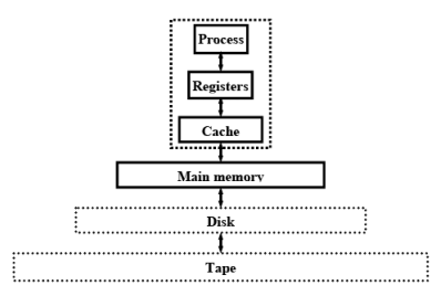
Fig. 6.1 The memory Hierarchy
Cache
- Usually designed with SRAM
- faster but more expensive than DRAM
- Usually on same chip as processor
- space limited, so much smaller than off-chip main memory
- faster access (1 cycle vs. several cycles for main memory)
- Cache operation
- Request for main memory access (read or write)
- First, check cache for copy
- cache hit
- copy is in cache, quick access - cache miss
- copy not in cache, read address and possibly its neighbors into cache
- Several cache design choices
- cache mapping, replacement policies, and write techniques
Cache Mapping
- is necessary as there are far fewer number of available cache addresses than the memory
- Are address’ contents in cache?
- Cache mapping used to assign main memory address to cache address and determine hit or miss
- Three basic techniques:
- Direct mapping
- Fully associative mapping
- Set-associative mapping
- Caches partitioned into indivisible blocks or lines of adjacent memory addresses
- usually 4 or 8 addresses per line
Direct Mapping
- Main memory address divided into 2 fields
- Index which contains
- cache address
- number of bits determined by cache size - Tag
- compared with tag stored in cache at address indicated by index
- if tags match, check valid bit
- Index which contains
- Valid bit
- indicates whether data in slot has been loaded from memory
- Offset
- used to find particular word in cache line
Fig. 6.2 Direct Mapping
Fully Associative Mapping
- Complete main memory address stored in each cache address
- All addresses stored in cache simultaneously compared with desired address
- Valid bit and offset same as direct mapping
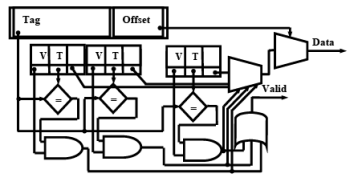
Fig. 6.3 Fully Associative Mapping
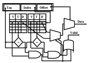
Set-Associative Mapping
- Compromise between direct mapping and fully associative mapping
- Index same as in direct mapping
- But, each cache address contains content and tags of 2 or more memory address locations
- Tags of that set simultaneously compared as in fully associative mapping
- Cache with set size N called N-way set-associative
- 2-way, 4-way, 8-way are common
Cache-Replacement Policy
- Technique for choosing which block to replace
- when fully associative cache is full
- when set-associative cache’s line is full
- Direct mapped cache has no choice
- Random
- replace block chosen at random
- LRU: least-recently used
- replace block not accessed for longest time
- FIFO: first-in-first-out
- push block onto queue when accessed
- choose block to replace by popping queue
Cache Write Techniques
- When written, data cache must update main memory
- Write-through
- write to main memory whenever cache is written to
- easiest to implement
- processor must wait for slower main memory write
- potential for unnecessary writes
- Write-back
- main memory only written when “dirty” block replaced
- extra dirty bit for each block set when cache block written to
- reduces number of slow main memory writes
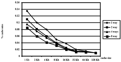
Cache Impact on System Performance
- Most important parameters in terms of performance:
- Total size of cache
- total number of data bytes cache can hold
- tag, valid and other house keeping bits not included in total - Degree of associativity
- Data block size
- Total size of cache
- Larger caches achieve lower miss rates but higher access cost
- e.g.,
- 2 Kbyte cache: miss rate = 15%, hit cost = 2 cycles, miss cost = 20 cycles
- avg. cost of memory access
= (0.85 * 2) + (0.15 * 20) = 4.7 cycles
- e.g.,
- 4 Kbyte cache: miss rate = 6.5%, hit cost = 3 cycles, miss cost will not change
- avg. cost of memory access = (0.935 * 3) + (0.065 * 20) = 4.105 cycles (improvement) - 8 Kbyte cache: miss rate = 5.565%, hit cost = 4 cycles, miss cost will not change
- avg. cost of memory access = (0.94435 * 4) + (0.05565 * 20) = 4.8904 cycles
Cache Performance Trade-Offs
- Improving cache hit rate without increasing size
- Increase line size
- Change set-associativity
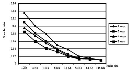
Fig. 6.5 Cache Performance
Advanced RAM
- DRAMs commonly used as main memory in processor based embedded systems
- high capacity, low cost
- Many variations of DRAMs proposed
- need to keep pace with processor speeds
- FPM DRAM: fast page mode DRAM
- EDO DRAM: extended data out DRAM
- SDRAM/ESDRAM: synchronous and enhanced synchronous DRAM
- RDRAM: rambus DRAM
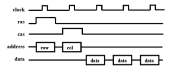
Basic DRAM
- Address bus multiplexed between row and column components
- Row and column addresses are latched in, sequentially, by strobing ras (row address strobe) and cas (column address strobe) signals, respectively
- Refresh circuitry can be external or internal to DRAM device
- strobes consecutive memory address periodically causing memory content to be refreshed
- Refresh circuitry disabled during read or write operation
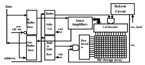
Fig. 6.6 The Basic Dynamic RAM Structure
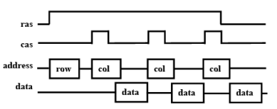
Fast Page Mode DRAM (FPM DRAM)
- Each row of memory bit array is viewed as a page
- Page contains multiple words
- Individual words addressed by column address
- Timing diagram:
- row (page) address sent
- 3 words read consecutively by sending column address for each
Extra cycle eliminated on each read/write of words from same
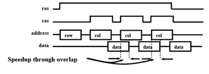
Extended data out DRAM (EDO DRAM)
- Improvement of FPM DRAM
- Extra latch before output buffer
- allows strobing of cas before data read operation completed
- Reduces read/write latency by additional cycle
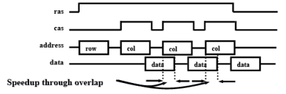
Fig. 6.8 The timing diagram in EDORAM
(S)ynchronous and Enhanced Synchronous (ES) DRAM
- SDRAM latches data on active edge of clock
- Eliminates time to detect ras/cas and rd/wr signals
- A counter is initialized to column address then incremented on active edge of clock to access consecutive memory locations
- ESDRAM improves SDRAM
- added buffers enable overlapping of column addressing
- faster clocking and lower read/write latency possible
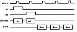
Fig. 6.9 The timing diagram in SDRAM
Rambus DRAM (RDRAM)
- More of a bus interface architecture than DRAM architecture
- Data is latched on both rising and falling edge of clock
- Broken into 4 banks each with own row decoder
- can have 4 pages open at a time
- Capable of very high throughput
DRAM Integration Problem
- SRAM easily integrated on same chip as processor
- DRAM more difficult
- Different chip making process between DRAM and conventional logic
- Goal of conventional logic (IC) designers:
- minimize parasitic capacitance to reduce signal propagation delays and power consumption - Goal of DRAM designers:
- create capacitor cells to retain stored information - Integration processes beginning to appear
Memory Management Unit (MMU)
- Duties of MMU
- Handles DRAM refresh, bus interface and arbitration
- Takes care of memory sharing among multiple processors
- Translates logic memory addresses from processor to physical memory addresses of DRAM
- Modern CPUs often come with MMU built-in
- Single-purpose processors can be used
Question
Q1. Discuss different types of cache mappings.
Ans:
Direct, Fully Associative, Set Associative
Q2 Discuss the size of the cache memory on the system performance.
Ans:
Q3. Discuss the differences between EDORAM and SDRAM
Ans:
EDO RAM
SDRAM
|
47 videos|77 docs|65 tests
|
FAQs on Memory - 2 - Embedded Systems (Web) - Computer Science Engineering (CSE)
| 1. What is memory and how does it work? |  |
| 2. What are the different types of memory? | |
| 3. How can I improve my memory? | |
| 4. What are the common causes of memory loss? | |
| 5. Can memory loss be prevented or reversed? | |


Viva Questions
,Memory - 2 | Embedded Systems (Web) - Computer Science Engineering (CSE)
,shortcuts and tricks
,Semester Notes
,Free
,Important questions
,Objective type Questions
,Extra Questions
,Memory - 2 | Embedded Systems (Web) - Computer Science Engineering (CSE)
,MCQs
,Previous Year Questions with Solutions
,Exam
,ppt
,video lectures
,study material
,Summary
,mock tests for examination
,Sample Paper
,Memory - 2 | Embedded Systems (Web) - Computer Science Engineering (CSE)
,practice quizzes
,past year papers
;


Memory - 2 Free PDF Download
Importance of Memory - 2
Memory - 2 Notes
Memory - 2 Computer Science Engineering (CSE) Questions
Study Memory - 2 on the App
|
© EduRev
|
Education Revolution
|


|


