Metal Oxide Field Effect Transistor | Analog and Digital Electronics - Electrical Engineering (EE) PDF Download

In the world of electronics, you all must have heard the term Transistor in your life at least once. But have you ever thought about what are transistors? How do they work? What are the types of transistors? So today you will get the answer to all such questions. In this article, we will understand about the device MOSFET and its characteristics. But before that let me clear the term transistor.
So a transistor is a type of semiconductor device that is used to maintain and regulate the voltage and current level. It has the functions of a switch and an amplifier. You might be thinking about what is the need to study transistors. This is because it is one of the essential components in most of the electronic devices present today. We cannot imagine this world of technology without transistors.
MOSFET Basics
MOSFET is a very popular kind of IG-FET. The full form of MOSFET is the Metal Oxide Semiconductor Field Effect Transistor. The diagram of MOSFET is given below.
In these kinds of devices, the gate terminal is separated from the channel using the insulating layer. This insulating layer is formed from the oxide layer of the semiconductor. The insulating layer of MOSFET is formed from SiO2.
What is MOSFET?
Now MOSFET is also classified into two types:-
1. Depletion type
2. Enhancement type
When we provide external voltage in the channel, it can either increase or decrease the amount of charge carriers in the channel. If the number of charge carriers increases, it is known as enhancement type MOSFET. But if the number of charge carriers decrease then it is known as depletion type MOSFET.
What is FET ?
Now one of those transistors is FET. The full form of FET is a Field Effect Transistor. It is a three-terminal device that uses the electric field to regulate and maintain the flow of current. The three terminals are :
- Gate
- Drain
- Source
Current flows between two terminals, drain and source. The flow of current can be controlled by applying external voltage between gate and source. This external voltage generates electric field in device. So by controlling electric field and voltage, we can regulate the flow of current. Thus it is a Voltage Controlled Device. It has many applications such as Integrated circuits, oscillators and buffer amplifiers. They are small in size and because of this they are used in ICs.
Now there are two types of FET:-
1. JFET ( Junction Field Effect Transistor)
2. IG-FET (Insulated Gate Field Effect Transistor)
Important Terminologies
- Transistor : It is a kind of semiconductor device which can generate electric current or voltage on its own.
- Gate Terminal : The current conduction between drain and source is controlled by applying voltage in the gate terminal.
- Threshold voltage : Maximum amount of voltage required for the formation of channel.
- p-channel : Channel made with p-type semiconductor.
- n-channel : Channel made with n-type semiconductor.
- Saturation : Level in which something becomes constant.
MOSFET Types
Now these enhancement type and depletion type MOSFET is further classified into p-channel and n-channel MOSFET.
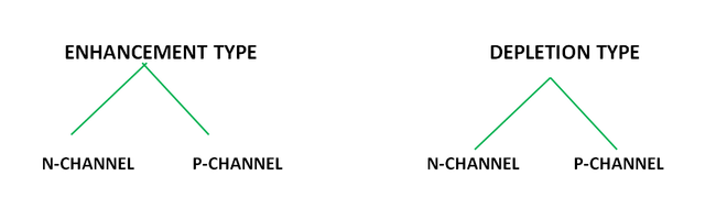
Types of MOSFET
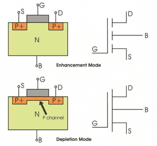
Enhancement Type MOSFET
- In this type of MOSFET, no channel is present from the beginning and hence no current flows.
- But when the +ve voltage more than the threshold voltage is applied, it leads to an enhancement of a channel between the drain and source due to the gate voltage and thus it results in the conductivity of device.
- They are mostly used in digital applications.
Depletion Type MOSFET
- In this type of MOSFET, channel is present from the beginning which means conduction of current is there.
- -ve voltage is applied to reduce the flow of current and this reduces the width of the channel.
- Not used commonly in devices.
Working Principle of MOSFET
MOSFET is a type of transistor in which conductivity depends upon the semiconductor channel across the drain and source terminal. This semiconductor channel may be p-channel or n-channel depending upon the configuration of the MOSFET.
A MOSFET consists of three terminals- drain, source and gate. By applying some voltage across gate and source, there forms a inversion layer or a channel between the drain and source if the voltage applied is threshold voltage. (Threshold voltage is the minimum required voltage for the conduction of current) . If the applied voltage is less than the threshold voltage, no channel is formed. Hence current cannot flow in the MOSFET. This situation is called as Cutoff region (OFF).
And after a certain level of voltage, the current becomes constant in the MOSFET. This condition is called as saturation point. MOSFET is a voltage controlled device so the thickness of channel and the amount of current depends upon the voltage applied across gate and source. If more voltage applied, width of channel increases and more amount of current able to flow through the device.
MOSFET Construction
MOSFET is a transistor which is used as switch or amplifier and in many other applications. The basic construction of MOSFET can be explained as below:-
- Substrate : MOSFET is constructed on a silicon wafer that is it acts as a base of the device.
- SiO2 : A thin layer of insulating material is formed with SiO2 for the exchange of electrons and holes.
- Gate Terminal : A gate terminal is formed on the insulating layer. This controls the flow of current between the drain and source with the help of gate voltage.
- Source and drain terminals : These are created on the either side of the gate. These are basically doped regions.
- Channel : Region between the gate, drain and source is known as channel which controls the flow of charge among them.
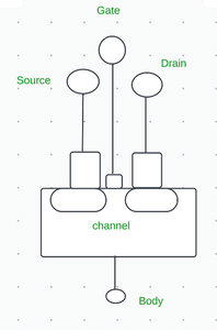
In the above figure, gate ,source and drain are he three terminals. Below are the two channels and body terminal.
MOSFET works in two modes-
1. Depletion Mode: The transistor requires the Gate-Source voltage (VGS) to switch the device “OFF”. The depletion-mode MOSFET is equivalent to a “Normally Closed” switch.
2. Enhancement Mode: The transistor requires a Gate-Source voltage (VGS) to switch the device “ON”. The enhancement mode MOSFET is equivalent to a “Normally Open” switch.
P-Channel MOSFET
The drain and source are heavily doped p+ region and the substrate is in n-type. The current flows due to the flow of positively charged holes, and that’s why known as p-channel MOSFET.
When we apply negative gate voltage, the electrons present beneath the oxide layer experience repulsive force and are pushed downward into the substrate, the depletion region is populated by the bound positive charges which are associated with the donor atoms.
The negative gate voltage also attracts holes from the P+ source and drain region into the channel region.
N-Channel MOSFET

The drain and source are heavily doped N+ region and the substrate is p-type. The current flows due to the flow of negatively charged electrons and that’s why known as n-channel MOSFET.
When we apply the positive gate voltage, the holes present beneath the oxide layer experience repulsive force, and the holes are pushed downwards into the bound negative charges which are associated with the acceptor atoms.
The positive gate voltage also attracts electrons from the N+ source and drain region into the channel thus an electron-rich channel is formed.
|
135 videos|167 docs|71 tests
|


video lectures
,Sample Paper
,past year papers
,ppt
,practice quizzes
,MCQs
,Previous Year Questions with Solutions
,Summary
,Semester Notes
,Extra Questions
,mock tests for examination
,Viva Questions
,Free
,Metal Oxide Field Effect Transistor | Analog and Digital Electronics - Electrical Engineering (EE)
,study material
,Metal Oxide Field Effect Transistor | Analog and Digital Electronics - Electrical Engineering (EE)
,Important questions
,Exam
,shortcuts and tricks
,Objective type Questions
,Metal Oxide Field Effect Transistor | Analog and Digital Electronics - Electrical Engineering (EE)
;


Metal Oxide Field Effect Transistor Free PDF Download
Importance of Metal Oxide Field Effect Transistor
Metal Oxide Field Effect Transistor Notes
Metal Oxide Field Effect Transistor Electrical Engineering (EE) Questions
Study Metal Oxide Field Effect Transistor on the App
|
© EduRev
|
Education Revolution
|


|


