Operational Amplifier | Electrical Engineering SSC JE (Technical) - Electrical Engineering (EE) PDF Download
OPERATIONAL AMPLIFIER
1st Stage : Difference amplifier.
2nd Stage : High gain linear amplifier.
3rd Stage : Emitter follower.
4th Stage : DC level shifter and output amplifier.
Ideal Op–amp Characteristics
1. Input resistance is infinite, Zin = ¥ , so no current enters the input terminal.
2. A zero output resistance, Zout = 0.
3. Infinite voltage gain, Av = ¥ .
4. Characteristics do not drift with temperature.
Inverting Amplifier
Input Impedance The input resistance is equal to resistance Z.
Unity Follower
The output signal is in phase with the input signal and of same magnitude.
Input impedance is very high, so it provides very good isolation between stages.
Summing amplifier
Differential amplifier
differentiator
Integrator
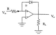
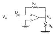
Precision Rectifier Main defect with Si rectifier is its cut in voltage of 0.7 V and so, voltages less than this value cannot be rectified. This defect is over come in op-amp rectifiers and voltages in the mill volt range can be obtained.
when Vs is + ve diode is ON and feedback loop is established and Vo follows Vs.
When Vs is – ve, diode is OFF and feedback loop is open and Vo =0
All Pass filter
Band Pass Filter
Check what type of filter is given circuit by just inspection putting w = 0 (capacitor open–circuit) and w = ¥ (capacitor short–circuit) In above circuit when w = 0 , C1 = open circuit and Vo = 0 V, similar for w = ¥ (C1 = C2) so it does not passes high as well as low frequency so it is band pass.
Non - Inverting Integration
Double Integration
Clamper : In some situation it may be necessary to raise or lower reference voltage, which is done by adding or subtracting a dc voltage to the original reference voltage of 0.
Two Type of Clamper Circuit:
(a) If the d.c. level added is positive, it is positive, it is positive clamper.
(b) If the d.c. level is lowered and negative, its negative clamper.
Positive Clamper sm V =Vsin wt, for negative swing D conducts and capacitor charge to peak value Vm and cathode end to capacitor is positive
Vo =Vs + Vc (or Vm) = 2 Vm for positive swing and 0 for negative swing
Logarithmic Amplifiers

- When Vin < 0; diode is off, Op-amp behaves as comparator . At this time Vo = + Vsat
- WhenVin > 0 diode is ON Vo =– 0.7 V For small range of Vin. It behaves as logarithmic amplifier.

Antilogarithmic Amplifier


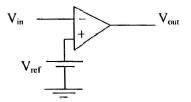
Comparator In a comparator, the level of the applied input voltage is compared with a known reference voltage:
1. As a comparator, the level of the applied input voltage is compared with a known reference voltage.
2. As a comparator, the Op-amp are operated in the open condition without feedback resistor.
3. Since it is operated in open loop condition, the assumption (V+ =V– = Vd = o) is not applicable.
4. Open loop gain is very high, so output goes to saturation levels ( ± Vcc) even for very low inputs.
5. If 1 or 2V drops in Rc’s of the transistor of the differential stage, the saturation voltage will be ( ± 13V) for a supply voltage of ( ± 15V) .

If (V2–V1) = Vin > 0, Vo = + Vsat
If (V2 – V1) = Vin < 0, Vo = – Vsat
Zero Crossing Comparator and Detector


With sinusoidal, we obtain rectangular pulse waveform at the output. Output remains at + Vsat or –Vsat till the input voltage is above or below Vref.
Vin > Vref : Vout = – Vsat Vin < Vref : Vout = Vsat
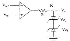
Output remains at ± Vsat ( ± 13) is not suitable for TTL operation. We can clamp the output voltage to lowest value by connecting at the output zener diodes back to back.

Vin > Vref : Vo = (VD + VZI) Vin < Vref: Vo = – (VD + VZI) With VD = 0.7,
For positive Vo, Dz2 act as a diode and for negative V0, DzI acts as a simple diode.
R restricts the current to the operating point of zener.
This circuit is known as by - phase amplifier:
Slew Rate It is defined as the maximum time rate of change of the output voltage (dvo/dt)max.
Describes the large signal limitation of the opamp.
For faithful reproduction of this sinusoid requires wVm £ slew rate where,Vm = peak amplitude of applied signal w = frequency of input signal.
Timing Circuit Digital systems require some kind of a timing waveform for example, a source of trigger pulses, for clocked sequential systems. Rectangular waveform is most desirable. The generators of rectangular waveforms are referred to as multivibrators.
Three Types of Multivibrator
1. Astable (or free running) multivibrator.
2. Monostable multivibrator (one-shot), and
3. Bistable multivibrator (or flip-flop).
1. Astable multivibrator is nothing but an oscillator, which generates rectangular waveform. It has two quasi-stable states, and doesnot require any triggering; hence it is referred to as a free running multivibrator.
2. Monostable Multivibrator: has one stable state i.e. under steady state condition, its output is fixed it is either in the low or the high state. When the circuit is triggered with an externally applied pulse it goes into the other state, i.e. if it was in low state, it will go to high and vice-versa. The circuit remains in this state for the elements used in the circuit.
3. Bistable Multivibrator: A multivibrator circuit in which both the states are stable is referred to as a bistable multivibrator or FF. This circuit makes transition pulse is applied.
|
23 videos|94 docs|42 tests
|
FAQs on Operational Amplifier - Electrical Engineering SSC JE (Technical) - Electrical Engineering (EE)
| 1. What is an operational amplifier (op-amp) in electrical engineering? |  |
| 2. How does an operational amplifier work? |  |
| 3. What are the characteristics of an ideal operational amplifier? |  |
| 4. How can an operational amplifier be used as an inverting amplifier? |  |
| 5. What are some common applications of operational amplifiers? |  |


