Physics Exam  >  Physics Notes  >  Solid State Physics, Devices & Electronics  >  P-N Junction Diode: Assignment

P-N Junction Diode: Assignment | Solid State Physics, Devices & Electronics PDF Download

Q.1. An abrupt p-n junction diode is formed with two sides of resistivities 2 Ωcm in the p -side and 1 Ωcm on the n-side at temperature 300 K . Find the height of the potential energy barrier for Ge. (μn = 3800 cm2/Vs, μP = 1800 cm2/Vs, and ni = 2.5x1013 cm-3

P-N Junction Diode: Assignment | Solid State Physics, Devices & Electronics


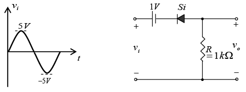
Q.2. Draw output waveforms for the circuit given below.
P-N Junction Diode: Assignment | Solid State Physics, Devices & Electronics

Let id = 0 and vd = -0.7V.
For transition voltage, apply KVL in input section
-vi + 1 - 0.7 + 0 = 0 ⇒ v= 0.3V = VT
Thus if vi < 0.3 V, diode is ON and if vi > 0.3V, diode is OFF.
If v= 0
0 + 1 - 0.7 + v0 = 0 ⇒ v0 = -0.3V
If vi = -5V
+ 5 + 1 - 0.7 + v0 = 0 ⇒ v= -5.3V


Q.3. A diode at room temperature (kT = 0.025eV )with a current of 1μA has a forward bias voltage VF = 0.4V. Find the diode current when VF = 0.5.

P-N Junction Diode: Assignment | Solid State Physics, Devices & Electronics


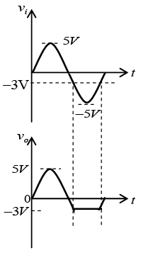
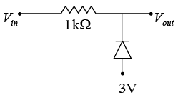
Q.4. A sine wave of 5V amplitude is applied at the input of the circuit shown in the figure. Draw output waveforms for the circuit given below. (Assume diode is ideal)
P-N Junction Diode: Assignment | Solid State Physics, Devices & Electronics

If Vin > -3V, diode is OFF and V0 = Vin.
If Vin < -3V, diode is ON and V0 = -3V

P-N Junction Diode: Assignment | Solid State Physics, Devices & Electronics


Q.5. (a) Consider a Si diode with η = 1.5 . Find the change in voltage if the current changes from 0.1 mA to 10 mA at 300 K.
(b) Consider a Si diode with η = 1 has v = 0.7V at i = 1 mA . Find the voltage drop at i = 0.1 mA and i = 10 mA at 300 K.

P-N Junction Diode: Assignment | Solid State Physics, Devices & Electronics

P-N Junction Diode: Assignment | Solid State Physics, Devices & Electronics


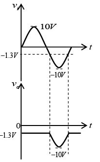
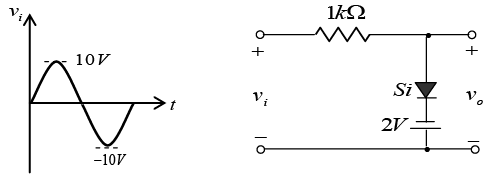
Q.6. Draw output waveforms for the circuit given below.
P-N Junction Diode: Assignment | Solid State Physics, Devices & Electronics

Let id = 0 and vd = 0.7V.
For transition voltage, apply KVL in input section -vi + 0 + 0.7 - 2 = 0 ⇒ vi = -1.3V = VT 
Thus if vi > -1.3V, diode is ON then v0 = -1.3V and if vi < -1.3V, diode is OFF.
v0 = vi
P-N Junction Diode: Assignment | Solid State Physics, Devices & Electronics


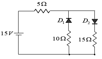
Q.7. The circuit shown in figure has two oppositely connected ideal diodes in parallel. Assume diodes are ideal.
P-N Junction Diode: Assignment | Solid State Physics, Devices & Electronics

(a) Find current through diode D1.
(b) Find current through diode D2.

Diode D1 is OFF and diode D2 is ON.
Thus current through diode D1 is 0 A and
Thus current through diode D2 is P-N Junction Diode: Assignment | Solid State Physics, Devices & Electronics


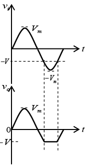
Q.8. Draw output waveforms for the circuit given below take |Vm| >|V|.
(Assume diodes to be ideal)
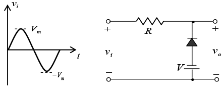
P-N Junction Diode: Assignment | Solid State Physics, Devices & Electronics

Let id = 0 and vd = 0V.
For transition voltage, apply KVL in input section -vi + 0 + 0 - V = 0 ⇒ vi = -V = VT 
Thus if vi > -V, diode is OFF then v0 =vi
and if vi < -V, diode is ON then v0 = -V.

P-N Junction Diode: Assignment | Solid State Physics, Devices & Electronics


Q.9. For the circuit shown in figure below  
(a) Find current through diode.
(b) Find output voltage Vo.
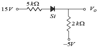
P-N Junction Diode: Assignment | Solid State Physics, Devices & Electronics

(a) Under given biasing condition diode is ON. Let current through 5 kΩ resistance 

is I.
Apply KVL in the input section,
-15 + I x 5k + 0.7 + I x 2k - 5 = 0 ⇒ I = (19.3/7) mA = 2.76mA
(b) V0 = 2.76 x 2 - 5 = 0.51V


Q.10. Draw output waveforms for the circuit given below (RC >> T/2).
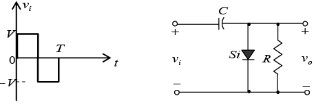
P-N Junction Diode: Assignment | Solid State Physics, Devices & Electronics

P-N Junction Diode: Assignment | Solid State Physics, Devices & Electronics


Q.11. In the following circuit, the voltage drop across the diode in forward bias condition ism 0.7 V. Find the current I and ID.
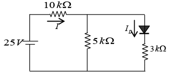
P-N Junction Diode: Assignment | Solid State Physics, Devices & Electronics

P-N Junction Diode: Assignment | Solid State Physics, Devices & ElectronicsApply KVL in two loops
-25 + I x 10 + (I-ID) x 5 = 0 ⇒ 15I - 5ID = 25 ...(i)
0.7 + ID x 3 -(I-ID) x 5 = 0 ⇒ 5I - 8ID = 0.7 ...(ii) 

From (i) and (ii), I = 2.06 mA and ID = 1.21mA.


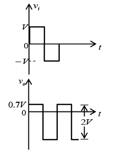
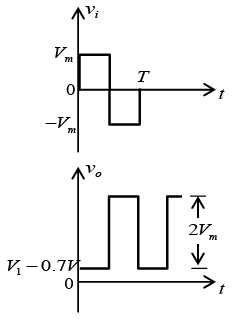
Q.12. Draw output waveforms for the circuit given below (RC >> T/2). Take |Vm| > |V1|.

P-N Junction Diode: Assignment | Solid State Physics, Devices & Electronics

P-N Junction Diode: Assignment | Solid State Physics, Devices & Electronics


Q.13. The I - V characteristics of the diode in the circuit below is given by
P-N Junction Diode: Assignment | Solid State Physics, Devices & Electronics

where V is measured in volts and I is measured in amperes. 
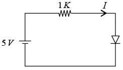
P-N Junction Diode: Assignment | Solid State Physics, Devices & Electronics

Find the current I in the circuit.

Applying K.V.L.
-5 + 1000 x I + V = 0 ⇒ -5 + 1000 x (V - 0.7)/500 +V = 0
⇒ -5 + 2 (V - 0.7) + V = 0 ⇒ 3V = 6.4 ⇒ V = 2.13 Volts
Thus I = (V - 0.7)/500 = (2.13 - 0.7)/500 = 1.43/500 = 2.86 mA


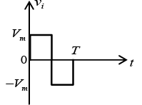
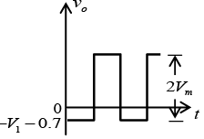
Q.14. Draw output waveforms for the circuit given below (RC >> T/2). Take |Vm| > |V1|.

P-N Junction Diode: Assignment | Solid State Physics, Devices & Electronics

P-N Junction Diode: Assignment | Solid State Physics, Devices & Electronics

P-N Junction Diode: Assignment | Solid State Physics, Devices & Electronics


Q.15. An a.c. supply of 220 V, 50 Hz is applied to a half wave rectifier circuit through a transformer of turn ratio 5 :1 . The forward resistance of the diode is 100 Ω and the load 

resistance is 5 kΩ.
(a) Find output d.c. voltage.
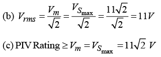
(b) Find r.ms. value of the output voltage.
(c) What should be PIV rating of the diode?

P-N Junction Diode: Assignment | Solid State Physics, Devices & Electronics

P-N Junction Diode: Assignment | Solid State Physics, Devices & Electronics


Q.16. Consider the circuit shown in figure below.
(a) Find the maximum Zener current IZ,max, when RL = 2kΩ.
(b) Find the minimum Zener current IZ,min, when RL = 4kΩ.
(c) Find IL and IZ with Vin = 22V and RL = 2kΩ.
(d) Find the power dissipated across the Zener when RL = 5kΩ and Vin = 20V.
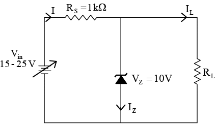
P-N Junction Diode: Assignment | Solid State Physics, Devices & Electronics

P-N Junction Diode: Assignment | Solid State Physics, Devices & Electronics
P-N Junction Diode: Assignment | Solid State Physics, Devices & Electronics ⇒ PZ = VZIZ = 10 x 8 = 80mW


Q.17 For the rectifier circuit shown in the figure, the sinusoidal voltage ( V1 or V2) at the output of the transformer has a maximum value of 10 V. The load resistance RL is 2 kΩ.
(a) Find the average current Iav through the resistor RL.
(b) Find the rms current Irms through the resistor RL.
(c) What should be PIV rating of the diode?
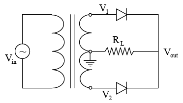
P-N Junction Diode: Assignment | Solid State Physics, Devices & Electronics

(a) P-N Junction Diode: Assignment | Solid State Physics, Devices & Electronics
(b) P-N Junction Diode: Assignment | Solid State Physics, Devices & Electronics
(c) PIV Rating ≥ 2V= 20V


Q.18. A variable power supply (5V - 20V) is connected to a Zener diode specified by a breakdown voltage of 10 V (see figure).
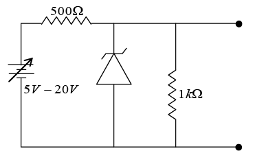
P-N Junction Diode: Assignment | Solid State Physics, Devices & Electronics

(a) The ratio of the maximum power to the minimum power dissipated across the load 

resistor.

(b) Find the minimum power dissipated across the zener diode.
(c) Find the maximum power dissipated across the zener diode.

(a) When V = 5V ⇒ open circuit voltage Vi = P-N Junction Diode: Assignment | Solid State Physics, Devices & Electronics 

P-N Junction Diode: Assignment | Solid State Physics, Devices & Electronics
When V = 20V ⇒ open circuit voltage Vi = P-N Junction Diode: Assignment | Solid State Physics, Devices & Electronics
P-N Junction Diode: Assignment | Solid State Physics, Devices & Electronics

(b) When V = 5V ⇒ open circuit voltage P-N Junction Diode: Assignment | Solid State Physics, Devices & Electronics 

⇒ Pz,min = VZIZ = 0.
(c) When V = 20V ⇒ open circuit voltage P-N Junction Diode: Assignment | Solid State Physics, Devices & Electronics
P-N Junction Diode: Assignment | Solid State Physics, Devices & Electronics
⇒ Pz,max = VZIZ = 10 x 10 = 100mW


Q.19. An a.c. voltage of 220 V , 50 Hz is applied to the primary of a 20 :1 step down transformer. The secondary of the transformer is bridge type and connected to a full wave rectifier with a load resistance 500Ω. Forward resistance of the diode is 10Ω.
(a) Find output d.c. voltage.
(b) Find r.ms. value of the output voltage.
(c) What should be PIV rating of the diode?

P-N Junction Diode: Assignment | Solid State Physics, Devices & Electronics
P-N Junction Diode: Assignment | Solid State Physics, Devices & Electronics 


Q.20. The figure below shows the current voltage characteristics of a diode over a range of voltage and current where it is safe to operate the diode. 
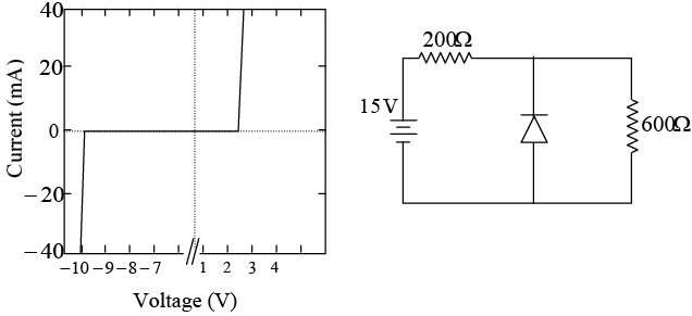
P-N Junction Diode: Assignment | Solid State Physics, Devices & Electronics(a) Find the approximate diode current, in mA .
(b) Find the approximate current, in mA , through the 600 Ω resistance.
(c) Find the approximate current, in mA , through the 200 Ω resistance.

Characteristics shows that the diode used is a zener diode.
(a) Open circuit voltage P-N Junction Diode: Assignment | Solid State Physics, Devices & Electronics
P-N Junction Diode: Assignment | Solid State Physics, Devices & Electronics 
(b) Open circuit voltage P-N Junction Diode: Assignment | Solid State Physics, Devices & Electronics
P-N Junction Diode: Assignment | Solid State Physics, Devices & Electronics
(c) Open circuit voltage P-N Junction Diode: Assignment | Solid State Physics, Devices & Electronics
⇒ I= 5/0.2 = 25mA

The document P-N Junction Diode: Assignment | Solid State Physics, Devices & Electronics is a part of the Physics Course Solid State Physics, Devices & Electronics.
All you need of Physics at this link: Physics
91 videos|21 docs|25 tests

FAQs on P-N Junction Diode: Assignment - Solid State Physics, Devices & Electronics

1. What is a P-N junction diode?
Ans. A P-N junction diode is a two-terminal device formed by joining a P-type semiconductor and an N-type semiconductor. It is the simplest form of a semiconductor device and acts as a one-way valve for the flow of electric current.
2. How does a P-N junction diode work?
Ans. When a P-N junction diode is forward-biased, meaning the P-side is connected to the positive terminal of a battery and the N-side is connected to the negative terminal, the majority carriers (holes in P-type and electrons in N-type) move towards the junction, allowing current flow. In reverse bias, the majority carriers are pushed away from the junction, creating a depletion region where no current flows.
3. What is the forward voltage drop of a P-N junction diode?
Ans. The forward voltage drop of a P-N junction diode is typically around 0.6 to 0.7 volts for silicon diodes and 0.2 to 0.3 volts for germanium diodes. This voltage drop is necessary to overcome the potential barrier at the junction and allow current to flow.
4. What are the applications of P-N junction diodes?
Ans. P-N junction diodes have various applications in electronics. Some common applications include rectification of AC to DC current, voltage clamping, voltage regulation, signal modulation and demodulation, and as temperature sensors. They are also used in solar cells and light-emitting diodes (LEDs).
5. What is the breakdown voltage of a P-N junction diode?
Ans. The breakdown voltage of a P-N junction diode is the reverse voltage at which the diode starts conducting in the reverse bias direction. It is an important parameter to consider for diodes used in high-voltage applications. The breakdown voltage can be different for different types of diodes and can range from a few volts to several thousand volts.
91 videos|21 docs|25 tests
Download as PDF
Explore Courses for Physics exam
Signup for Free!
Signup to see your scores go up within 7 days! Learn & Practice with 1000+ FREE Notes, Videos & Tests.
10M+ students study on EduRev
Related Searches

Previous Year Questions with Solutions

,

shortcuts and tricks

,

Devices & Electronics

,

Free

,

P-N Junction Diode: Assignment | Solid State Physics

,

Exam

,

P-N Junction Diode: Assignment | Solid State Physics

,

MCQs

,

P-N Junction Diode: Assignment | Solid State Physics

,

Sample Paper

,

ppt

,

pdf

,

Viva Questions

,

mock tests for examination

,

study material

,

Semester Notes

,

Important questions

,

practice quizzes

,

Devices & Electronics

,

Devices & Electronics

,

past year papers

,

video lectures

,

Extra Questions

,

Objective type Questions

,

Summary

;