Electrical Engineering (EE) Exam  >  Electrical Engineering (EE) Notes  >  Analog and Digital Electronics  >  Previous Year Questions- Operational Amplifiers - 3

Previous Year Questions- Operational Amplifiers - 3 | Analog and Digital Electronics - Electrical Engineering (EE) PDF Download

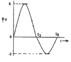
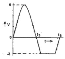
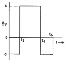
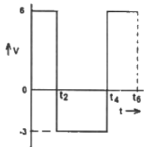
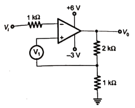
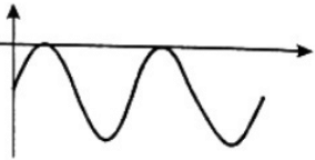
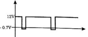
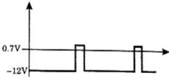
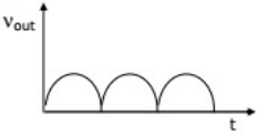
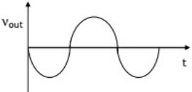
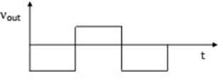
Q31: An ideal op-amp circuit and its input wave form as shown in the figures. The output waveform of this circuit will be (2009)
Previous Year Questions- Operational Amplifiers - 3 | Analog and Digital Electronics - Electrical Engineering (EE)(a) Previous Year Questions- Operational Amplifiers - 3 | Analog and Digital Electronics - Electrical Engineering (EE)(b) Previous Year Questions- Operational Amplifiers - 3 | Analog and Digital Electronics - Electrical Engineering (EE)(c) Previous Year Questions- Operational Amplifiers - 3 | Analog and Digital Electronics - Electrical Engineering (EE)(d) Previous Year Questions- Operational Amplifiers - 3 | Analog and Digital Electronics - Electrical Engineering (EE)Ans:
(d)
Sol: Previous Year Questions- Operational Amplifiers - 3 | Analog and Digital Electronics - Electrical Engineering (EE)When Vi < V1(upto t2); Vo = +ve
When V> V1(t2 ≤ t ≤ t4); Vo = −ve
Previous Year Questions- Operational Amplifiers - 3 | Analog and Digital Electronics - Electrical Engineering (EE)
Q32: Transformer and emitter follower can both be used for impedance matching at the output of an audio amplifier. The basic relationship between the input power Pin and output power Pout in both the cases is (2009)
(a) Pin=PoutPin = Pout for both transformer and emitter follower
(b) Pin>PoutPin > Pout for both transformer and emitter follower
(c) Pin < Pout for transformer and Pin = Pout for emitter follower
(d) Pin=PoutPin = Pout for transformer and Pin < Pout for emitter follower
Ans:
(d)
Sol: For emitter follower
AV ≅ 1; Ais high
⇒ AP = AV⋅AI is high ⇒ Pout > Pin
For transformer, Pin = Pout

Q33: The following circuit has R = 10kΩ, C = 10μF. The input voltage is a sinusoidal at 50 Hz with an rms value of 10 V. Under ideal conditions, the current is from the source is (2009)
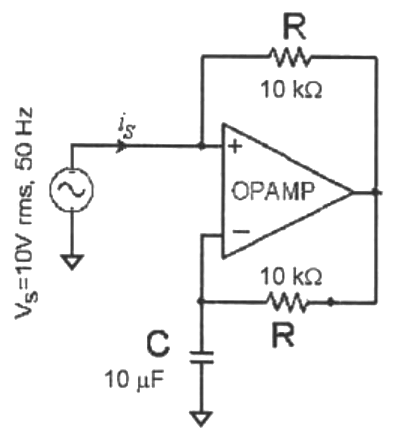
Previous Year Questions- Operational Amplifiers - 3 | Analog and Digital Electronics - Electrical Engineering (EE)(a) 10π mA leading by 90%
(b) 20π mA leading by 90%
(c) 10 mA leading by 90%
(d) 10π mA lagging by 90%
Ans:
(d)
Sol: Previous Year Questions- Operational Amplifiers - 3 | Analog and Digital Electronics - Electrical Engineering (EE)Is = −VsjωC
= −j(10 × 2π × 50 × 10 × 10−6)
= −j10π...mA
= 10π mA lagging by 90°

Q34: The nature of feedback in the op-amp circuit shown is (2009)
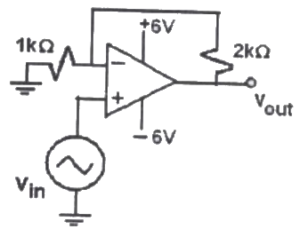
Previous Year Questions- Operational Amplifiers - 3 | Analog and Digital Electronics - Electrical Engineering (EE)(a) Current-Current feedback
(b) Voltage-Voltage feedback
(c) Current-Voltage feedback
(d) Voltage-Current feedback
Ans: 
(b)
Sol: Voltage-series feedback arrangement or voltage-voltage feedback.

Q35:A general filter circuit is shown in the figure :
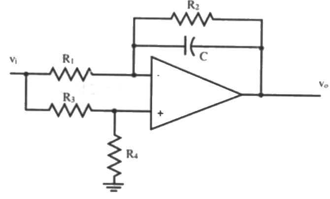
Previous Year Questions- Operational Amplifiers - 3 | Analog and Digital Electronics - Electrical Engineering (EE) The output of the above circuit is given to the circuit shown below in figure :
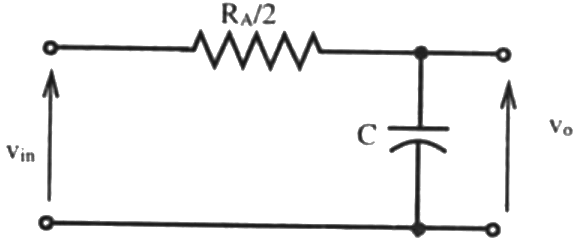
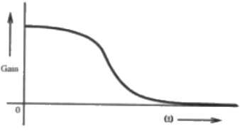
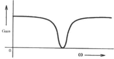
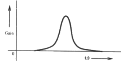
Previous Year Questions- Operational Amplifiers - 3 | Analog and Digital Electronics - Electrical Engineering (EE)The gain v/s frequency characteristic of the output (vo) will be (2008)
(a) Previous Year Questions- Operational Amplifiers - 3 | Analog and Digital Electronics - Electrical Engineering (EE)(b) Previous Year Questions- Operational Amplifiers - 3 | Analog and Digital Electronics - Electrical Engineering (EE)(c) Previous Year Questions- Operational Amplifiers - 3 | Analog and Digital Electronics - Electrical Engineering (EE)(d) Previous Year Questions- Operational Amplifiers - 3 | Analog and Digital Electronics - Electrical Engineering (EE)Ans:
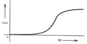
(d)
Sol: Previous Year Questions- Operational Amplifiers - 3 | Analog and Digital Electronics - Electrical Engineering (EE)Which is similar to equation of a band pass filter.

Q36: A general filter circuit is shown in the figure :
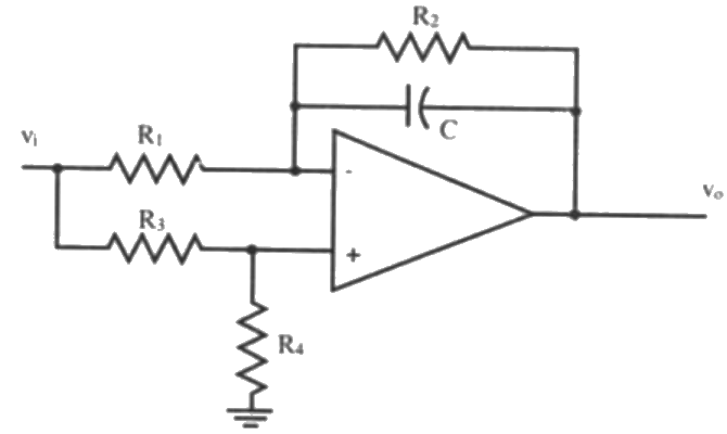
Previous Year Questions- Operational Amplifiers - 3 | Analog and Digital Electronics - Electrical Engineering (EE) If R1 = R2 = RA and R3 = R4 = RB, the circuit acts as a (2008)
(a) all pass filter
(b) band pass filter
(c) high pass filter
(d) low pass filter
Ans:
(c)
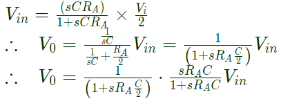
Sol: Previous Year Questions- Operational Amplifiers - 3 | Analog and Digital Electronics - Electrical Engineering (EE)Let, Vi only on onverting terminal
Previous Year Questions- Operational Amplifiers - 3 | Analog and Digital Electronics - Electrical Engineering (EE)Here, Previous Year Questions- Operational Amplifiers - 3 | Analog and Digital Electronics - Electrical Engineering (EE)

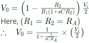
Let, Vonly only on non-inverting terminal  

Previous Year Questions- Operational Amplifiers - 3 | Analog and Digital Electronics - Electrical Engineering (EE)Putting the value of Rf, we get
Previous Year Questions- Operational Amplifiers - 3 | Analog and Digital Electronics - Electrical Engineering (EE)So, it is high pass filter.

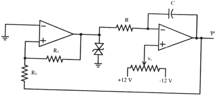
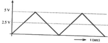
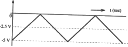
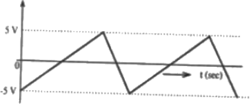
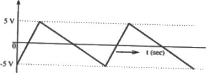
Q37: A waveform generator circuit using OPAMPs is shown in the figure. It produces a triangular wave at point 'P' with a peak to peak voltage of 5 V for v= 0V.
Previous Year Questions- Operational Amplifiers - 3 | Analog and Digital Electronics - Electrical Engineering (EE) If the voltage vi is made +2.5 V, the voltage waveform at point 'P' will become (2008)
(a)
Previous Year Questions- Operational Amplifiers - 3 | Analog and Digital Electronics - Electrical Engineering (EE) (b) Previous Year Questions- Operational Amplifiers - 3 | Analog and Digital Electronics - Electrical Engineering (EE)(c) Previous Year Questions- Operational Amplifiers - 3 | Analog and Digital Electronics - Electrical Engineering (EE)(d) Previous Year Questions- Operational Amplifiers - 3 | Analog and Digital Electronics - Electrical Engineering (EE)Ans:
(a)

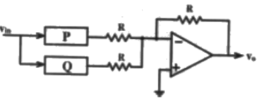
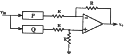
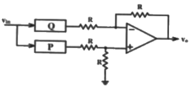
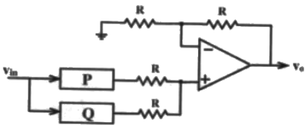
Q38: The block diagrams of two of half wave rectifiers are shown in the figure. The transfer characteristics of the rectifiers are also shown within the block.
Previous Year Questions- Operational Amplifiers - 3 | Analog and Digital Electronics - Electrical Engineering (EE)It is desired to make full wave rectifier using above two half-wave rectifiers. The resultants circuit will be (2008)
(a) Previous Year Questions- Operational Amplifiers - 3 | Analog and Digital Electronics - Electrical Engineering (EE)(b) Previous Year Questions- Operational Amplifiers - 3 | Analog and Digital Electronics - Electrical Engineering (EE)(c) Previous Year Questions- Operational Amplifiers - 3 | Analog and Digital Electronics - Electrical Engineering (EE)(d) Previous Year Questions- Operational Amplifiers - 3 | Analog and Digital Electronics - Electrical Engineering (EE)Ans:
(b)
Sol: For (Vin > 0),
P → V01 = negative
Q → V02 = 0
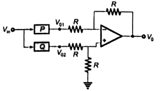
Previous Year Questions- Operational Amplifiers - 3 | Analog and Digital Electronics - Electrical Engineering (EE)V0 will be positive due to inverting action.
For (Vin < 0),
P → V′01 = 0
Q → V′02 = positive
Vwill be positive due to non-inverting action. So, output is always rectified.

Q39: The switch S in the circuit of the figure is initially closed, it is opened at time t = 0. You may neglect the zener diode forward voltage drops. What is the behavior of Vout for t > 0? (2007)
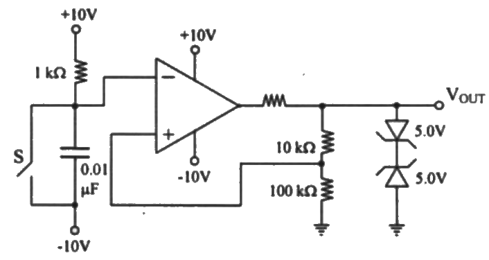
Previous Year Questions- Operational Amplifiers - 3 | Analog and Digital Electronics - Electrical Engineering (EE)(a) It makes a transition from -5 V to +5 V at t = 12.98 μs
(b) It makes a transition from -5 V to +5 V at t = 2.57 μs
(c) It makes a transition from +5 V to -5 V at t = 12.98 μs
(d) It makes a transition from +5 V to -5 V at t = 2.57 μs
Ans: 
(c)
Sol: Let the voltage at the non-inverting terminal of the opamp be Va volts and the voltage at inverting terminal be Vb volts.
At t = 0+ switch is open Vo = 5V and Vb = −10V
Previous Year Questions- Operational Amplifiers - 3 | Analog and Digital Electronics - Electrical Engineering (EE)As t → ∞, V→ 10 V
Vb = Vf+(Vi−Vf)e−t/RC....(i)
Putiing , V= (50/11) at t = T1
Vi = −10V and Vf = 10V in eq.(i)
We get, T= 12.98 μsec
∴ At t = 12.98μsec, Vchanges from 5V to -5V.  

Q40: The circuit shown in the figure is (2007)
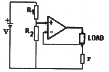
Previous Year Questions- Operational Amplifiers - 3 | Analog and Digital Electronics - Electrical Engineering (EE)(a) a voltage source with voltage Previous Year Questions- Operational Amplifiers - 3 | Analog and Digital Electronics - Electrical Engineering (EE)

(b) a voltage source with voltage Previous Year Questions- Operational Amplifiers - 3 | Analog and Digital Electronics - Electrical Engineering (EE)
(c) a current source with current Previous Year Questions- Operational Amplifiers - 3 | Analog and Digital Electronics - Electrical Engineering (EE)
(d) a current source with current Previous Year Questions- Operational Amplifiers - 3 | Analog and Digital Electronics - Electrical Engineering (EE)
Ans: (d)
Sol: It behaves as current source because the output current Idepends upon (Vin) and resistance only.
Where, Previous Year Questions- Operational Amplifiers - 3 | Analog and Digital Electronics - Electrical Engineering (EE)


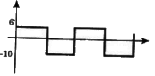
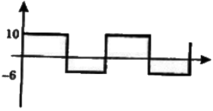
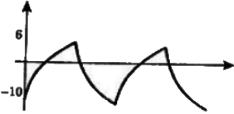
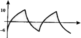
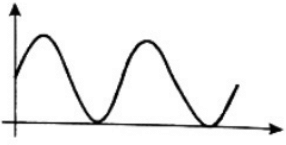
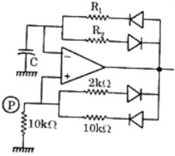
Q41: A relaxation oscillator is made using OPAMP as shown in figure. The supply voltages of the OPAMP are ±12 V. The voltage waveform at point P will be (2006)
Previous Year Questions- Operational Amplifiers - 3 | Analog and Digital Electronics - Electrical Engineering (EE)(a) Previous Year Questions- Operational Amplifiers - 3 | Analog and Digital Electronics - Electrical Engineering (EE)(b) Previous Year Questions- Operational Amplifiers - 3 | Analog and Digital Electronics - Electrical Engineering (EE)(c) Previous Year Questions- Operational Amplifiers - 3 | Analog and Digital Electronics - Electrical Engineering (EE)(d) Previous Year Questions- Operational Amplifiers - 3 | Analog and Digital Electronics - Electrical Engineering (EE)Ans:
(a)
Sol: Output will be either at +Vsat or −Vsat. When output will be at +Vsat diodde connected to 10kΩ resistance will be on making voltage at point P equal to 6V.
When output will be at −Vsat diodde connected to 2kΩ resistance will be on making voltage at point P equal to -10V.


Q42: For a given sinusoidal input voltage, the voltage waveform at point P of the clamper circuit shown in figure will be (2006)
Previous Year Questions- Operational Amplifiers - 3 | Analog and Digital Electronics - Electrical Engineering (EE)(a) Previous Year Questions- Operational Amplifiers - 3 | Analog and Digital Electronics - Electrical Engineering (EE)(b) Previous Year Questions- Operational Amplifiers - 3 | Analog and Digital Electronics - Electrical Engineering (EE)(c) Previous Year Questions- Operational Amplifiers - 3 | Analog and Digital Electronics - Electrical Engineering (EE)(d) Previous Year Questions- Operational Amplifiers - 3 | Analog and Digital Electronics - Electrical Engineering (EE)Ans:
(d)
Sol: For -ve half of the input +ve terminal of OPAMP is at higher potential than -ve terminal and output goes to +Vsat but due to this high potential diode gets on and restricts the output to 0.7V only.
And for +ve half of the input +ve terminal of OPAMP is at lower potential than -ve terminal's potential and output goes to −Vsat and remains at −Vsat.

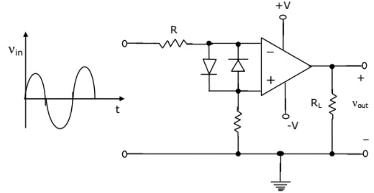
Q43: In the given figure, if the input is a sinusoidal signal, the output will appear as shown (2005)
Previous Year Questions- Operational Amplifiers - 3 | Analog and Digital Electronics - Electrical Engineering (EE) (a) Previous Year Questions- Operational Amplifiers - 3 | Analog and Digital Electronics - Electrical Engineering (EE)(b) Previous Year Questions- Operational Amplifiers - 3 | Analog and Digital Electronics - Electrical Engineering (EE)(c) Previous Year Questions- Operational Amplifiers - 3 | Analog and Digital Electronics - Electrical Engineering (EE)(d) Previous Year Questions- Operational Amplifiers - 3 | Analog and Digital Electronics - Electrical Engineering (EE)Ans:
(c)
Sol: Output will be at its saturation values and it is having a phase difference of (180°).
For +ve half of the input, first diode will be on making -ve terminal of op-amp to 0.7V larger than the voltage at +ve input, so output will be −Vsat.
For -ve half of the input reverse of the above will happen and output will go +Vsat.

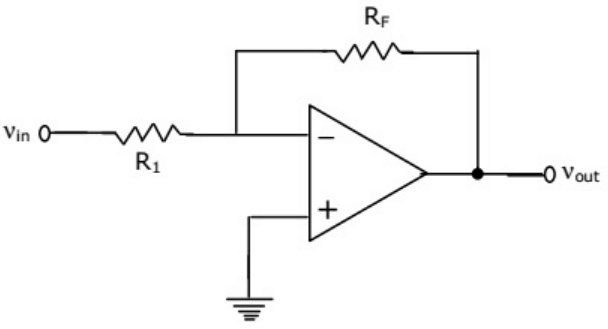
Q44: Consider the inverting amplifier, using an ideal operational amplifier shown in the figure. The designer wishes to realize the input resistance seen by the smallsignal source to be as large as possible, while keeping the voltage gain between -10 and -25. The upper limit on RF is 1 MΩ. The value of R1 should be (2005)
Previous Year Questions- Operational Amplifiers - 3 | Analog and Digital Electronics - Electrical Engineering (EE)(a) Infinity
(b) 1MΩ
(c) 100kΩ
(d) 40kΩ
Ans: 
(d)
Sol: Previous Year Questions- Operational Amplifiers - 3 | Analog and Digital Electronics - Electrical Engineering (EE)If gain = -25 then Previous Year Questions- Operational Amplifiers - 3 | Analog and Digital Electronics - Electrical Engineering (EE)

If gain = -10 then Previous Year Questions- Operational Amplifiers - 3 | Analog and Digital Electronics - Electrical Engineering (EE)

So if we keep R1 to be 100kΩ then we never get the gain -25 for any Rso we can keep R1 to be 40kΩ.


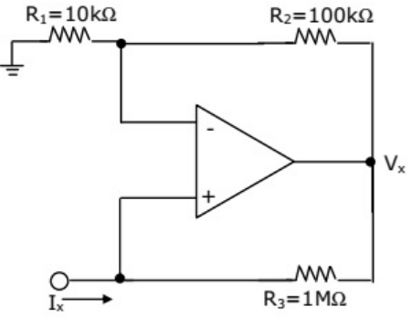
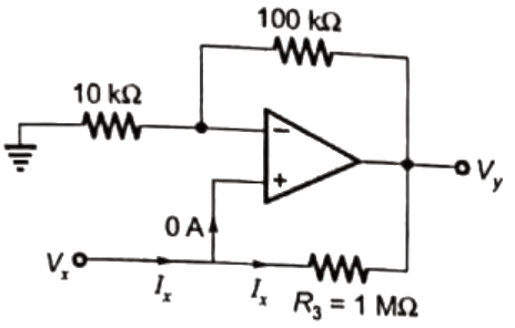
Q45: The input resistance  Previous Year Questions- Operational Amplifiers - 3 | Analog and Digital Electronics - Electrical Engineering (EE) of the circuit in figure is (2004)
Previous Year Questions- Operational Amplifiers - 3 | Analog and Digital Electronics - Electrical Engineering (EE)(a) +100kΩ
(b) 100kΩ−100kΩ
(c) +1MΩ
(d) −1MΩ
Ans:
(b)
Sol: Previous Year Questions- Operational Amplifiers - 3 | Analog and Digital Electronics - Electrical Engineering (EE)Here, Previous Year Questions- Operational Amplifiers - 3 | Analog and Digital Electronics - Electrical Engineering (EE)

But, Previous Year Questions- Operational Amplifiers - 3 | Analog and Digital Electronics - Electrical Engineering (EE)Previous Year Questions- Operational Amplifiers - 3 | Analog and Digital Electronics - Electrical Engineering (EE)

Q46: Assuming the operational amplifier to be ideal, the gain Vout/Vin for the circuit shown in figure is (2004)
Previous Year Questions- Operational Amplifiers - 3 | Analog and Digital Electronics - Electrical Engineering (EE)(a) -1
(b) -20
(c) -100
(d) -120
Ans: 
(d)
Sol: Using KCL at node 1, we have,
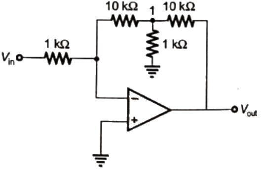
Previous Year Questions- Operational Amplifiers - 3 | Analog and Digital Electronics - Electrical Engineering (EE)Previous Year Questions- Operational Amplifiers - 3 | Analog and Digital Electronics - Electrical Engineering (EE)12V1 = Vout   ...(i)
Also, using KCL at inverting node, we get
Previous Year Questions- Operational Amplifiers - 3 | Analog and Digital Electronics - Electrical Engineering (EE)V1 = −Vin × 10 ...(ii)  
From equation (i) and (ii), we get
Previous Year Questions- Operational Amplifiers - 3 | Analog and Digital Electronics - Electrical Engineering (EE)
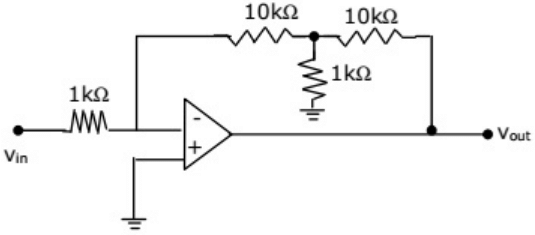
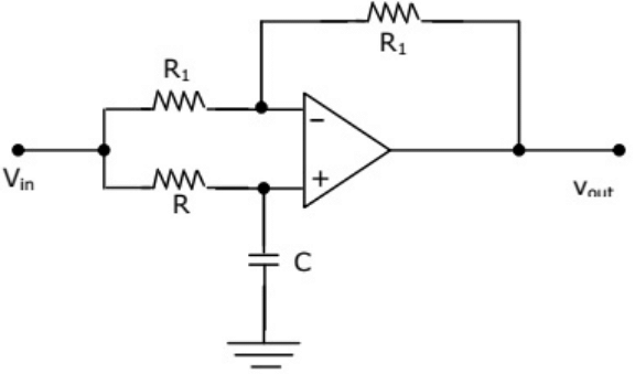
Q47: For the circuit of figure with an ideal operational amplifier, the maximum phase shift of the output Vout with reference to the input Vin is (2003)
Previous Year Questions- Operational Amplifiers - 3 | Analog and Digital Electronics - Electrical Engineering (EE)(a) 0°
(b) -90°
(c) +90°
(d) ±180°
Ans: 
(d)
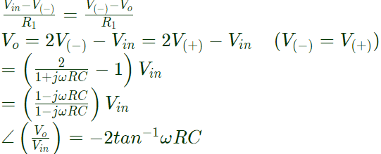
Sol:Previous Year Questions- Operational Amplifiers - 3 | Analog and Digital Electronics - Electrical Engineering (EE)where, V(−) = V(+) [For ideal Op-amp]
Previous Year Questions- Operational Amplifiers - 3 | Analog and Digital Electronics - Electrical Engineering (EE) For −90° ≤ θ ≤ 90°, maximum phase shift occurs (+180°).  

Q48: An op-amp, having a slew rate of 62.8 V/μsec, is connected in a voltage follower configuration. If the maximum amplitude of the input sinusoid is 10V, then the minimum frequency at which the slew rate limited distortion would set in at the output is (2001)
(a) 1 MHz
(b) 6.28 MHz
(c) 10 MHz
(d) 62.8 MHz
Ans:
(a)
Sol: S.R. = ωVm
62.8V/μs = 2πf × 10
Previous Year Questions- Operational Amplifiers - 3 | Analog and Digital Electronics - Electrical Engineering (EE)
The document Previous Year Questions- Operational Amplifiers - 3 | Analog and Digital Electronics - Electrical Engineering (EE) is a part of the Electrical Engineering (EE) Course Analog and Digital Electronics.
All you need of Electrical Engineering (EE) at this link: Electrical Engineering (EE)
137 videos|143 docs|71 tests

Top Courses for Electrical Engineering (EE)

FAQs on Previous Year Questions- Operational Amplifiers - 3 - Analog and Digital Electronics - Electrical Engineering (EE)

1. What is an operational amplifier (op-amp) and how does it work?
Ans. An operational amplifier (op-amp) is a high-gain electronic voltage amplifier with differential input and usually a single-ended output. It amplifies the voltage difference between its two inputs. The op-amp's output voltage is typically hundreds of thousands of times larger than the voltage difference between its input terminals.
2. What are the different configurations in which an op-amp can be used?
Ans. Op-amps can be used in various configurations such as an inverting amplifier, non-inverting amplifier, summing amplifier, difference amplifier, integrator, differentiator, voltage follower, etc. Each configuration has its unique characteristics and applications.
3. What are the ideal characteristics of an op-amp?
Ans. The ideal characteristics of an op-amp include infinite open-loop gain, infinite input impedance, zero output impedance, infinite bandwidth, and zero input offset voltage. While real op-amps do not achieve these ideal characteristics, they come close in practical applications.
4. How can negative feedback be used in op-amp circuits?
Ans. Negative feedback is commonly used in op-amp circuits to stabilize the gain, reduce distortion, improve bandwidth, and enhance the overall performance of the circuit. It involves feeding a portion of the output signal back to the input with an opposite polarity to the input signal.
5. What is the significance of the slew rate in op-amps?
Ans. The slew rate of an op-amp is the maximum rate of change of the output voltage per unit of time. It indicates the op-amp's ability to respond to rapid changes in the input signal. A higher slew rate allows the op-amp to accurately reproduce fast-changing input signals without distortion.
137 videos|143 docs|71 tests
Download as PDF
Explore Courses for Electrical Engineering (EE) exam

Top Courses for Electrical Engineering (EE)

Signup for Free!
Signup to see your scores go up within 7 days! Learn & Practice with 1000+ FREE Notes, Videos & Tests.
10M+ students study on EduRev
Related Searches

Exam

,

Previous Year Questions with Solutions

,

pdf

,

Previous Year Questions- Operational Amplifiers - 3 | Analog and Digital Electronics - Electrical Engineering (EE)

,

Important questions

,

Viva Questions

,

practice quizzes

,

study material

,

Previous Year Questions- Operational Amplifiers - 3 | Analog and Digital Electronics - Electrical Engineering (EE)

,

Sample Paper

,

mock tests for examination

,

Free

,

past year papers

,

MCQs

,

Semester Notes

,

shortcuts and tricks

,

Previous Year Questions- Operational Amplifiers - 3 | Analog and Digital Electronics - Electrical Engineering (EE)

,

Summary

,

Objective type Questions

,

ppt

,

video lectures

,

Extra Questions

;