Sallen Key Filter | Analog and Digital Electronics - Electrical Engineering (EE) PDF Download
The Sallen and Key Filter design is a second-order active filter topology which we can use as the basic building blocks for implementing higher order filter circuits, such as low-pass (LPF), high-pass (HPF) and band-pass (BPF) filter circuits.
As we have seen in this filters section, electronic filters, either passive or active, are used in circuits where a signals amplitude is only required over a limited range of frequencies. The advantage of using Sallen-Key Filter designs is that they are simple to implement and understand.
The Sallen and Key topology is an active filter design based around a single non-inverting operational amplifier and two resistors, thus creating a voltage-controlled voltage-source (VCVS) design with filter characteristics of, high input impedance, low output impedance and good stability, and as such allows individual Sallen-key filter sections to be cascaded together to produce much higher order filters.
But before we look at the design and operation of the Sallen-key filter, let’s first remind ourselves of the characteristics of a single resistor-capacitor, or RC network when subjected to a range of input frequencies.
The Voltage Divider
When two (or more) resistors are connected together across a DC supply voltage, different voltage values will be developed across each resistor creating what is basically called a voltage divider or potential divider network.
Resistive Voltage Divider
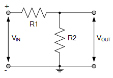
The basic circuit shown consists of two resistors in series connected across an input voltage, VIN.
Ohm’s Law tells us that the voltage dropped across a resistor is the sum of the current flowing through it multiplied by its resistive value, V = I*R, so if the two resistors are equal, then the voltage dropped across both resistors, R1 and R2 will also be equal and is split equally between them.
The voltage developed or dropped across resistor R2 represents the output voltage, VOUT and is given by the ratio of the two resistors and the input voltage. Thus the transfer function for this simple voltage divider network is given as:
Resistive Voltage Divider Transfer Function
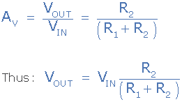
But what would happen to the output voltage, VOUT if we changed the input voltage to an AC supply or signal, and varied its frequency range. Well actually nothing, as resistors are generally not affected by changes in frequency (wirewounds excluded) so their frequency response is zero, allowing AC, Irms2*R voltages to be developed or dropped across the resistors just the same as it would be for steady state DC voltages.
The RC Voltage Divider
If we change resistor R1 above to a capacitor, C as shown, how would that affect our previous transfer function. We know from our tutorials about Capacitors that a capacitor behaves like an open circuit once charged when connected to a DC voltage supply.
RC Voltage Divider
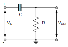
Thus when a steady state DC supply is connected to VIN, the capacitor will be fully charged after 5 time constants (5T = 5RC) and in which time it draws no current from the supply. Therefore there is no current flowing through the resistor, R and no voltage drop developed across it, so no output voltage. In other words, capacitors block steady state DC voltages once charged.
If we now change the input supply to an AC sinusoidal voltage, the characteristics of this simple RC circuit completely changes as the DC or constant part of the signal is blocked. So now we are analysing the RC circuit in the frequency domain, that is the part of the signal that depends on time.
In an AC circuit, a capacitor has the property of capacitive reactance, XC but we can still analyse the RC circuit in the same way as we did with the resistor only circuits, the difference is that the impedance of the capacitor now depends on frequency.
For AC circuits and signals, capacitive reactance (XC), is the opposition to alternating current flow through a capacitor measured in Ohm’s. Capacitive reactance is frequency dependant, that is at low frequencies (ƒ ≅ 0) the capacitor behaves like an open circuit and blocks them.
At very high frequencies (ƒ ≅ ∞) the capacitor behaves like a short circuit and pass the signals directly to the output as VOUT = VIN. However, somewhere in between these two frequency extremes the capacitor has an impedance given by XC. So our voltage divider transfer function from above becomes:

Thus changes in frequency, causes changes in XC, which causes changes in the magnitude of the output voltage. Consider the circuit below.
RC Filter Circuit
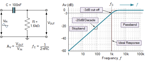
The graph shows the frequency response of this simple 1st-order RC circuit. At low frequencies the voltage gain is extremely low, as the input signal is being block by the reactance of the capacitor. At high frequencies the voltage gain is high (unity) as the reactance is causes the capacitor to effectively become a short-circuit to these high frequencies, so VOUT = VIN
However, there becomes a frequency point where the reactance of the capacitor is equal to the resistance of the resistor, that is: XC = R and this is called the “critical frequency” point, or more commonly called the cut-off frequency, or corner frequency ƒC.
As the cut-off frequency occurs when XC = R the standard equation used to calculate this critical frequency point is given as:
Cut-off Frequency Equation

The cut-off frequency, ƒC defines where the circuit, in this example, changes from attenuating or blocking all frequencies below, ƒC and starts to pass all the frequencies above this ƒC point. Thus the circuit is called a “high pass filter”.
The cut-off frequency is where the ratio of the input-to-output signal has a magnitude of 0.707 and when converted to decibels is equal to –3dB. This is often referred to as a filters 3dB down point.
As the reactance of the capacitor is related to frequency, that is capacitive reactance (XC) varies inversely with applied frequency, we can modify the above voltage divider equation to obtain the transfer function of this simple RC high pass filter circuit as shown.
RC Filter Circuit
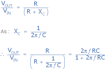
One of the main disadvantages of an RC filter is that the output amplitude will always be less than the input so it can never be greater than unity. Also the external loading of the output by more RC stages or circuits will have an affect on the filters characteristics. One way to overcome this problem is to convert the passive RC filter into an “Active RC Filter” by adding an operational amplifier to the basic RC configuration.
By adding an operational amplifier, the basic RC filter can be designed to provide a required amount of voltage gain at its output, thus changing the filter from an attenuator to an amplifier. Also due to the high input impedance and low output impedance of an operational amplifier prevents external loading of the filter allowing it to be easily adjusted over a wide frequency range without altering the designed frequency response.
Consider the simple active RC high-pass filter below.
Active High Pass Filter
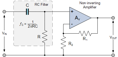
The RC filter part of the circuit responds the same as above, that is passing high frequencies but blocking low frequencies, with the cut-off frequency set by the values of R and C. The operational amplifier, or op-amp for short, is configured as a non-inverting amplifier whose voltage gain is set by the ratio of the two resistors, R1 and R2.
Then the closed loop voltage gain, AV in the passband of a non-inverting operational amplifier is given as:
Cut-off Frequency Equation

RC Filter Example
A simple 1st-order active high-pass filter is require to have a cut-off frequency of 500Hz and a passband gain of 9dB. Calculate the required components assuming a standard 741 operational amplifier is used.
From above we have seen that the cut-off frequency, ƒC is determined by the values of R and C in the frequency-selective RC circuit. If we assume a value for R of 5kΩ (any reasonable value would do), then the value of C is calculated as:
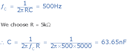
The calculated value of C is 63.65nF, so the nearest preferred value used is 62nF.
The gain of the high pass filter in the passband region is to be +9dB which equates to a voltage gain, AV of 2.83. Assume an arbitrary value for feedback resistor, R1 of 15kΩ, this gives a value for resistor R1 of:
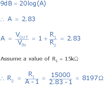
Again the calculated value of R2 is 8197Ω. The nearest preferred value would be 8200Ω or 8.2kΩ. This then gives us the final circuit for our active high-pass filter example of:
High Pass Filter Circuit
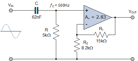
We have seen that a simple first-order high-pass filters can be made using a single resistor and capacitor producing a cut-off frequency, ƒC point where the output amplitude is –3dB down from the input amplitude. By adding a second RC filter stage to the first, we can convert the circuit into a second-order high-pass filter.
Second-order RC Filter
The simplest second order RC filter consists of two RC sections cascade together as shown. However, for this basic configuration to operate correctly, input and output impedances of the the two RC stages should not affect each others operation, that is they should be non-interacting.
High Pass Filter Circuit
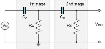
Cascading one RC filter stage with another (identical or different RC values), does not work very well because each successive stage loads the previous one and when more RC stages are added, the cut-off frequency point moves further away from the designed or required frequency.
One way to overcome this problem for a passive filter design is to have the input impedance of the second RC stage at least 10 times greater than the output impedance of the first RC stage. That is RB = 10*R1 and CB = CA/10 at the cut-off frequency.
The advantage of increasing the component values by a factor of 10 is that the resulting second-order filter produces a steeper roll-off of 40dB/decade than cascaded RC stages. But what if you wanted to design a 4th or a 6th-order filter, then the calculation of ten times the value of the previous components can be time consuming and complicated.
One simple way to cascade together RC filter stages which do not interact or load each other to create higher-order filters (individual filter sections need not be identical) which can be easily tuned and designed to provide required voltage gain is to use Sallen-key Filter stages.
Sallen and Key Filters
Sallen-Key is one of the most common filter configurations for designing first-order (1st-order) and second-order (2nd-order) filters and as such is used as the basic building blocks for creating much higher order filters.
The main advantages of the Sallen-key filter design are:
- Simplicity and Understanding of their Basic Design
- The use of a Non-inverting Amplifier to Increase Voltage Gain
- First and Second-order Filter Designs can be Easily Cascaded Together
- Low-pass and High-pass stages can be Cascaded Together
- Each RC stage can have a different Voltage Gain
- Replication of RC Components and Amplifiers
- Second-order Sallen-key Stages have Steep 40dB/decade roll-off than cascaded RC
However, there are some limitations to the basic Sallen-key filter design in that the voltage gain, AV and magnification factor, Q are closely related due to the use of an operational amplifier within the Sallen-key design.
Almost any Q value greater than 0.5 can be realised since using a non-inverting configuration, the voltage gain, AV will always be greater than 1, (unity) but must be less than 3 otherwise it will become unstable.
The simplest form of Sallen-key filter design is to use equal capacitor and resistor values (but the C’s and R’s don’t have to be equal), with the operational amplifier configured as a unity-gain buffer as shown. Note that resistor RA is no longer connected to ground but instead provides positive feedback for the amplifier.
Sallen-key High Pass Filter Circuit
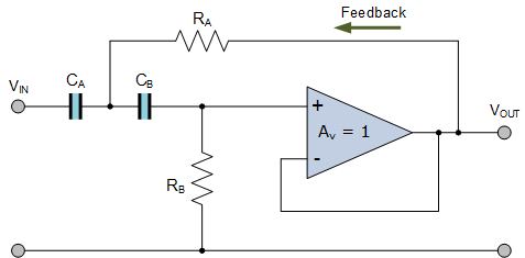
The passive components CA, RA, CB and RB form the second-order frequency-selective circuit.
Thus at low frequencies, capacitors CA and CB appear as open circuits, so the input signal is blocked resulting in no output. At higher frequencies, CA and CB appear to the sinusoidal input signal as short circuits, so the signal is buffered directly to the output.
However, around the cut-off frequency point, the impedance of CA and CB will be the same value as RA and RB, as noted above, so the positive feedback produced through CB provides voltage gain and and increase in output signal magnification, Q.
Since we now have two sets of RC networks, the above equation for the cut-off frequency for a Sallen-Key filter is modified too:
Sallen-key Cut-off Frequency Equation

If the two series capacitors CA and CB are made equal (CA = CB = C) and the two resistors RA and RB are also made equal (RA = RB = R), then the above equation simplifies to the original cut-off frequency equation of:

As the operational amplifier is configured as a unity gain buffer, that is A = 1, the cut-off frequency, ƒC and Q are completely independent of each other making for a simpler filter design. Then the magnification factor, Q is calculated as:

Therefore for the unity-gain buffer configuration, the voltage gain (AV) of the filter circuit is equal to 0.5, or -6dB (over damped) at the cut-off frequency point, and we would expect to see this because its a second-order filter response, as 0.7071*0.7071 = 0.5. That is -3dB*-3dB = -6dB.
However, as the value of Q determines the response characteristics of the filter, the proper selection of the operational amplifiers two feedback resistors, R1 and R2, allows us to select the required passband gain A for the chosen magnification factor, Q.
Note that for a Sallen-key filter topology, selecting the value of A to be very close to the maximum value of 3, will result in high Q values. A high Q will make the filter design sensitive to tolerance variations in the values of feedback resistors R1 and R2.
For example, setting the voltage gain to 2.9 (A = 2.9) will result in the value of Q being 10 (1/(3-2.9)), thus the filter becomes extremely sensitive around ƒC.
Sallen-key Filter Response
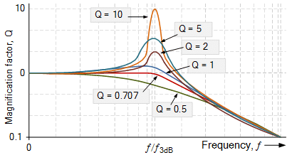
Then we can see that the lower the value of Q the more stable will be the Sallen and Key filter design. While high values of Q can make the design unstable, with very high gains producing a negative Q would lead to oscillations.
Sallen and Key Filter
Design a second-order high-pass Sallen and Key Filter circuit with the following characteristics: ƒC = 200Hz, and Q = 3
To simplify the math’s a little, we will assume that the two series capacitors CA and CB are equal (CA = CB = C) and also the two resistors RA and RB are equal (RA = RB = R).
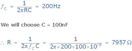
The calculated value of R is 7957Ω, so the nearest preferred value used is 8kΩ.
For Q = 3, the gain is calculated as:
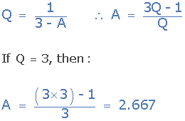
If A = 2.667, then the ratio of R1/R2 = 1.667 as shown.
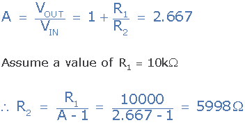
The calculated value of R2 is 5998Ω, so the nearest preferred value used 6000Ω or 6kΩ. This then gives us the final circuit for our Sallen and Key high-pass filter example of:
Sallen and Key High Pass Filter
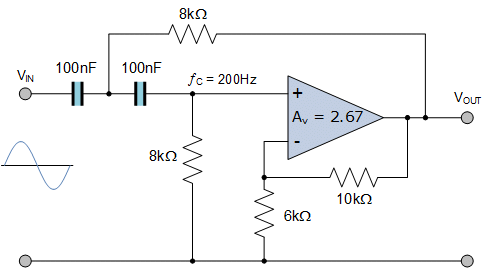
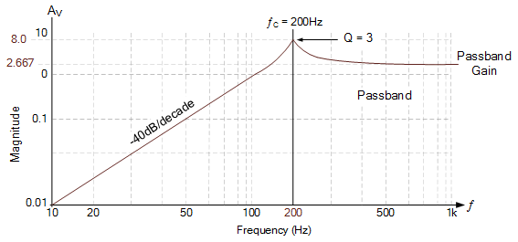
Then with a cut-off or corner frequency of 200Hz, a passband gain of 2.667, and a maximum voltage gain at the cut-off frequency of 8 (2.667*3) due to Q = 3, we can show the characteristics of this second-order high-pass Sallen and Key filter in the following Bode plot.
Sallen and Key Filter Bode Plot
Sallen and Key Filter Summary
We have seen here in this tutorial that the Sallen-Key configuration, also known as a voltage-controlled, voltage-source (VCVS) circuit is the most widely used filter topologies due mainly to the fact that the operational amplifier used within its design can be configured as a unity gain buffer or as a non-inverting amplifier.
The basic Sallen-key filter configuration can be used to implement different filter responses such as, Butterworth, Chebyshev, or Bessel with the correct selection of RC filter network. Most practical values of R and C can be used remembering that for a specific cut-off frequency point, the values of R and C are inversely proportional. That is as the value of R is made smaller, C becomes larger, and vice versa.
The Sallen-key is a 2nd-order filter design which can be cascaded together with other RC stages to create higher-order filters. Multiple filter stages need not be the same but can each have different cut-off frequency or gain characteristics. For instance, putting together a low-pass stage and a high-pass stage to create a Sallen and Key band-pass filter.
Here we have looked at designing a Sallen-key high-pass filter, but the same rules apply equally for a Sallen-key low-pass design. The voltage gain, AV of the op-amp determines its response. The voltage gain is preset by the two voltage divider resistors, R1 and R2 remembering that the voltage gain must always be less than 3 otherwise, the filter circuit will become unstable and oscillate.
|
135 videos|181 docs|71 tests
|


