Semiconductor Types | Analog and Digital Electronics - Electrical Engineering (EE) PDF Download
Semiconductor materials have some electrical properties that contribute to the operation of some electronic devices. In this, the resistivity falls as the temperature increases, whereas metal behaves differently in this term which is oppositely. It helps in the conduction of electricity in certain situations or conditions but not in all – the integrated circuits, transistors, and diodes all are made up of semiconductors. Apart from electricity conduction – it also functions to react to heat and light.
Holes and Electrons in Semiconductors
Holes and electronics are basically the charge carriers of the Semiconductor which results in the flow of current or electricity through it. Electrons, which carry a negative charge, orbit the nucleus of an atom. In semiconductors, they are assumed to be the primary carriers of electric charge. Within the semiconductor’s valence band, electrons are confined to atoms and exert limited influence on current flow. In a Semiconductor, when an electron leaves a place due to getting energy a place is left behind which is known as a hole. A hole in a Semiconductor represents a region of positive charge where an electron’s absence has left an opening in the covalent bond between atoms.
Classification of Semiconductors
Semiconductors can be classified as:
- Intrinsic Semiconductor
- Extrinsic Semiconductor
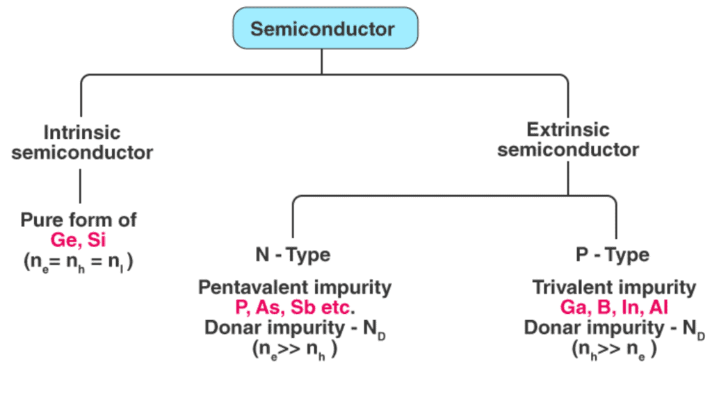
1. Intrinsic Semiconductors
- A pure form of semiconductor is called an intrinsic semiconductor. Conduction in an intrinsic semiconductors is either due to thermal excitation or crystal defects. Si and Ge are the two most important semiconductors used. Other examples include Gallium arsenide (GaAs), Indium Antimonide (InSb) etc.
- Let us consider the structure of Si. The atomic no. of Si is 14 and it has 4 valence electrons. These 4 electrons are shared by four neighbouring atoms in the crystal structure by means of covalent bond.
- Fig. 1.2a shows the crystal structure of Si at absolute zero temperature (0K). Hence a pure semiconductor has poor conductivity (due to lack of free electrons) at low or absolute zero temperature.
 Fig. 1.2a Crystal structure of Si at 0k
 - In fig.1.2b the valence electrons that jump into conduction band are called free electrons that are available for conduction.
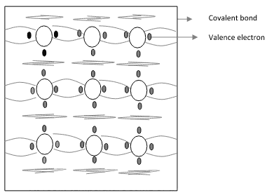
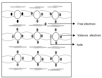 Fig. 1.2b Crystal Structure of Si at Room Temperature 0k
- The absence of electrons in covalent bond is represented by a small circle usually referred to as hole which is of positive charge. Even a hole serves as carrier of electricity in a manner similar to that of a free electron.
How do Intrinsic Semiconductors Work?
To understand the working mechanism of intrinsic semiconductors, we need to know the electronic configuration of their atoms.
The electronic configuration of silicon and germanium are:
1. Silicon –> 1s2 2s2 2p6 3s2 3p2
2. Germanium –> 1s2 2s2 2p6 3s2 3p6 4s2 3d10 4p2
We can clearly see that the outermost shell is having 4 electrons. At 0 Kelvin, the semiconductor behaves like a pure insulator. Now, with the increase in the temperature, electrons gain enough energy to free from its shell and leave behind an empty place known as a hole. Thus, a free electron is produced along with a hole. This is the reason for the equal number of electrons and holes in intrinsic semiconductors.
The mechanism by which a hole contributes to conductivity is explained as follows:
- When a bond is incomplete so that a hole exists, it is relatively easy for a valence electron in the neighbouring atom to leave its covalent bond to fill this hole. An electron moving from a bond to fill a hole moves in a direction opposite to that of the electron.
- This hole, in its new position, may now be filled by an electron from another covalent bond and the hole will correspondingly move one more step in the direction opposite to the motion of electron. Here we have a mechanism for conduction of electricity which does not involve free electrons.
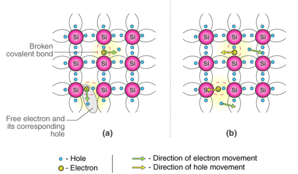 Conduction Mechanism in Case of Intrinsic Semiconductors (a) In absence of Electric Field (b) In presence of Electric Field
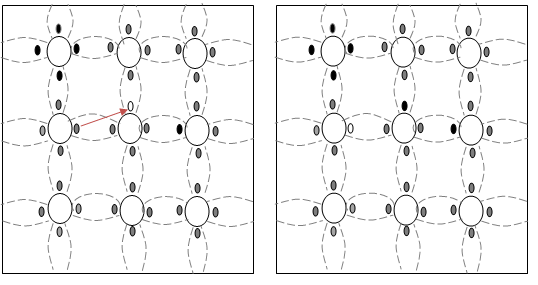 Fig 1.3 (a) & 1.3 (b)
- Fig 1.3a show that there is a hole at ion 6. Imagine that an electron from ion 5 moves into the hole at ion 6 so that the configuration of 1.3b results. If we compare both fig1.3a & fig 1.3b, it appears as if the hole has moved towards the left from ion 6 to ion 5. Further, if we compare fig 1.3b and fig 1.3c, the hole moves from ion 5 to ion 4.
- This discussion indicates that the motion of hole is in a direction opposite to that of motion of electron. Hence, we consider holes as physical entities whose movement constitutes flow of current.
- In a pure semiconductor, the number of holes is equal to the number of free electrons.
The Lattice of Pure Silicon Semiconductor at Different Temperatures
- At absolute zero Kelvin temperature: At this temperature, the covalent bonds are very strong and there are no free electrons and the semiconductor behaves as a perfect insulator.
- Above absolute temperature: With the increase in temperature few valence electrons jump into the conduction band and hence it behaves like a poor conductor.
Energy Band Diagram of Intrinsic Semiconductor
The energy band diagram of an intrinsic semiconductor is shown below:
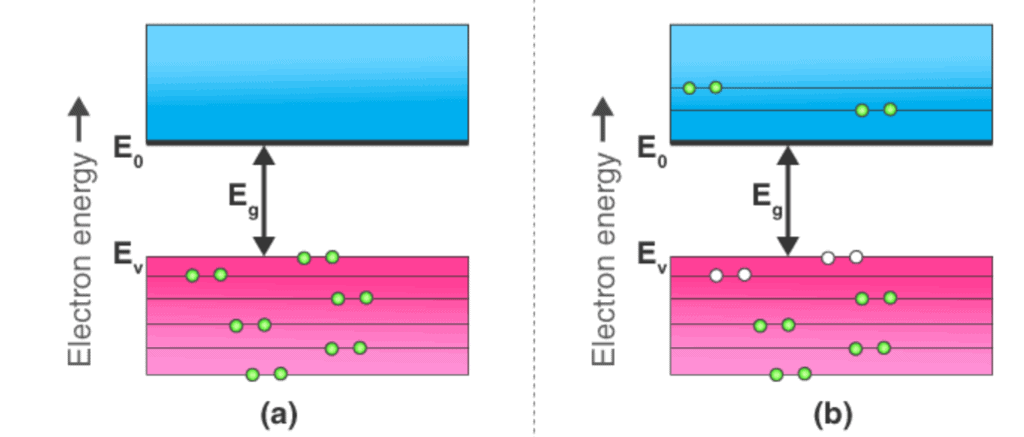
In intrinsic semiconductors, current flows due to the motion of free electrons as well as holes. The total current is the sum of the electron current Ie due to thermally generated electrons and the hole current IhTotal Current (I) = Ie + IhFor an intrinsic semiconductor, at finite temperature, the probability of electrons to exist in conduction band decreases exponentially with increasing bandgap
(Eg)n = n0e-Eg/2.Kb.where,
- Eg = Energy bandgap
- Kb = Boltzmann’s constant
2. Extrinsic Semiconductor
- Intrinsic semiconductor has very limited applications as they conduct very small amount of current at room temperature.
- The current conduction capability of intrinsic semiconductor can be increased significantly by adding small amounts of impurity to the intrinsic semiconductor.
- By adding impurities, it becomes impure or extrinsic semiconductor. This process of adding impurities is known as doping. The amount of impurity added is 1 part in 106 atoms.

(i) N-type Semiconductor
- If the added impurity is a pentavalent atom then the resultant semiconductor is called N-type semiconductor. Examples of pentavalent impurities are Phosphorus, Arsenic, Bismuth, Antimony etc.
- A pentavalent impurity has five valence electrons. Fig 1.3a shows the crystal structure of N-type semiconductor material where four out of five valence electrons of the impurity atom(antimony) forms covalent bond with the four intrinsic semiconductor atoms. The fifth electron is loosely bound to the impurity atom.
- This loosely bound electron can be easily excited from the valence band to the conduction band by the application of electric field or increasing the thermal energy. The energy required to detach the fifth electron form the impurity atom is very small of the order of 0.01eV for Ge and 0.05 eV for Si.
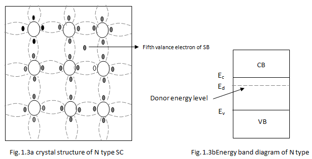
- The effect of doping creates a discrete energy level called donor energy level in the forbidden band gap with energy level Ed slightly less than the conduction band (fig 1.3b).
- The difference between the energy levels of the conducting band and the donor energy level is the energy required to free the fifth valence electron (0.01 eV for Ge and 0.05 eV for Si).
- At room temperature, almost all the electrons from the donor impurity atom are raised to conduction band and hence the number of electrons in the conduction band increases significantly. Thus, every antimony atom contributes to one conduction electron without creating a hole.
- In the N-type semiconductor, the no. of electrons increases and the no. of holes decreases compared to those available in an intrinsic semiconductor. The reason for decrease is the no. of holes is that the larger no. of electrons present increases the recombination of electrons with holes.
- Thus, current in N-type semiconductor is dominated by electrons which are referred to as majority carriers. Holes are the minority carriers in N-type semiconductor.
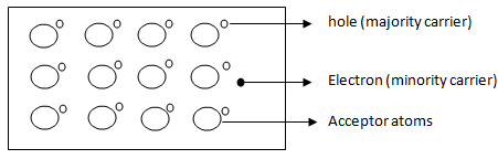
(ii) P-type Semiconductor
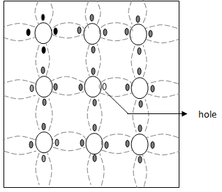
- If the added impurity is a trivalent atom, then the resultant semiconductor is called P-type semiconductor. Examples of trivalent impurities are Boron, Gallium, indium etc.
- The crystal structure of P-type semiconductor is shown in the fig1.3c. The three valence electrons of the impurity (boron) forms three covalent bonds with the neighboring atoms and a vacancy exists in the fourth bond giving rise to holes.
- The hole is ready to accept an electron from the neighbouring atoms. Each trivalent atom contributes to one hole generation and thus introduces a large no. of holes in the valence band.
- At the same time, the no. of electrons are decreased compared to those available in an intrinsic semiconductor because of increased recombination of holes and electrons. Fig. 1.3c Crystal structure of P-type Semiconductor
- Thus, in a P-type semiconductor, holes are majority carriers and electrons are minority carriers. Since each trivalent impurity atom is capable of accepting an electron, these are called acceptor atoms. The following fig 1.3d shows the pictorial representation of P-type semiconductor.
 Crystal Structure of P-type Semiconductor
- The conductivity of N-type semiconductor is greater than that of P-type semiconductor as the mobility of electron is greater than that of hole.
- For the same level of doping in N-type semiconductor and P-type semiconductor, the conductivity of an N-type semiconductor is around twice that of a P-type semiconductor.
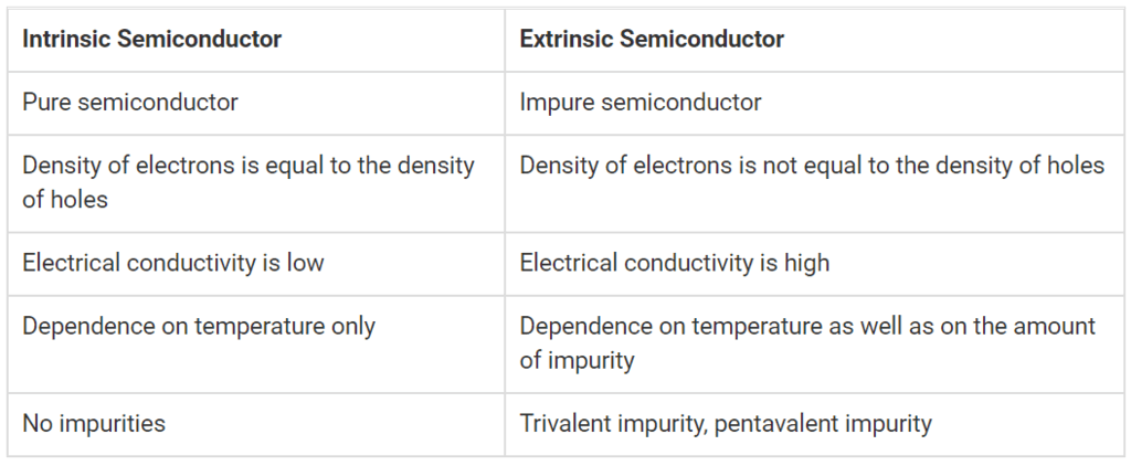
Difference between Intrinsic and Extrinsic Semiconductors
What is the Conductivity of Semiconductor?
- In a pure semiconductor, the number of holes is equal to the number of electrons. Thermal agitation continues to produce new electron-hole pairs and these electron-hole pairs disappear because of recombination.Intrinsic Semiconductor
- With each electron-hole pair created, two charge-carrying particles are formed. One is negative which is a free electron with mobility µn. The other is a positive i.e., hole with mobility µp. The electrons and hole move in the opposite direction in an electric field E, but since they are of opposite sign, the current due to each is in the same direction.
- Hence the total current density J within the intrinsic semiconductor is given by:
J = Jn + Jp
= q n µn E + q p µp E
= (n µn + p µp)qE
= σ E
Where n = No. of electrons/unit volume i.e., the concentration of free electrons
p = No. of holes/unit volume i.e., the concentration of holes
E = applied electric field strength, V/m
q = charge of electron or hole in Coulombs - Hence, σ is the conductivity of semiconductor which is equal to (n µn + p µp)q. The resistivity of semiconductor is reciprocal of conductivity.
Ρ = 1/ σ - It is evident from the above equation that current density within a semiconductor is directly proportional to applied electric field E.
- For a pure semiconductor, n = p = ni where ni = intrinsic concentration.
The value of ni is given by:
ni2 = AT3 exp (-EGO/KT)
Therefore, J = ni ( µn + µp) qE - Hence, conductivity in an intrinsic semiconductor is: σi = ni ( µn + µp) q
- Intrinsic conductivity increases at the rate of 5% per o C for Ge and 7% per o C for Si.

Conductivity in Extrinsic Semiconductor (N-Type and P-Type)

- The conductivity of an intrinsic semiconductor is given by:
σi = ni ( µn + µp) q
= (n µn + p µp)q - For N-type , n>>p
Therefore, σ = q n µn - For P-type, p>>n
Therefore, σ = q p µp
Fermi Level
- The highest energy level that an electron can occupy at the absolute zero temperature is known as the Fermi Level. The Fermi level lies between the valence band and conduction band because at absolute zero temperature the electrons are all in the lowest energy state.
- Due to lack of sufficient energy at 0 Kelvin, the Fermi level can be considered as the sea of fermions (or electrons) above which no electrons exist. The Fermi level changes as the solids are warmed and as electrons are added to or withdrawn from the solid.

Charge Densities in P-Type and N-Type Semiconductor
- Mass Action Law: Under thermal equilibrium for any semiconductor, the product of the no. of holes and the concentration of electrons is constant and is independent of the amount of donor and acceptor impurity doping.
n.p = ni2
where n = electron concentration
p = hole concentration
ni2= intrinsic concentration - In N-type semiconductor as the no. of electrons increase, the no. of holes decreases. Similarly in P-type, as the no. of holes increases the no. of electrons decreases. Thus, the product is constant and is equal to ni2 in case of intrinsic as well as extrinsic semiconductor.
- The law of mass action has given the relationship between free electrons concentration and hole concentration. These concentrations are further related by the law of electrical neutrality, as explained below.
[Question: 506293]
Law of Electrical Neutrality
- Semiconductor materials are electrically neutral. According to the law of electrical neutrality, in an electrically neutral material, the magnitude of positive charge concentration is equal to that of negative charge concentration.
- Let us consider a semiconductor that has ND donor atoms per cubic centimetre and NA acceptor atoms per cubic centimetre i.e., the concentration of donor and acceptor atoms are ND and NA, respectively.
- Therefore, ND positively charged ions per cubic centimetre are contributed by donor atoms and NA negatively charged ions per cubic centimetre are contributed by the acceptor atoms. Let n, p be concentration of free electrons and holes respectively. Then according to the law of neutrality,
ND + p = NA + n ...eq 1.1
For N-type semiconductor, NA = 0 and n>>p.
Therefore, ND ≈ n ...eq 1.2 - Hence for N-type semiconductor, the free electron concentration is approximately equal to the concentration of donor atoms. In later applications since some confusion may arise as to which type of semiconductor is under consideration at the given moment, the subscript n or p is added for N-type or P-type respectively. Hence eq 1.2 becomes ND ≈ nn.
- Therefore, the current density in N-type semiconductor is J = ND µn q E
and conductivity σ = ND µn q. - For P-type semiconductor, ND = 0 and p>>n.
Therefore NA ≈ p or NA ≈ pp. - Hence for P-type semiconductor, the hole concentration is approximately equal to the concentration of acceptor atoms.
Current density in N-type semiconductor is J = NA µp q E
And conductivity σ = NA µp q - Mass action law for N-type:
nn pn= ni2
pn = ni2/ ND since (nn≈ ND) - Mass action law for P-type:
np pp = ni2
np= ni2/ NA since (pp≈ NA)
GATE PYQs
Q1: Select the CORRECT statements regarding semiconductor devices [2022]
(a) Electrons and holes are of equal density in an intrinsic semiconductor at equilibrium.
(b) Collector region is generally more heavily doped than Base region in a BJT.
(c) Total current is spatially constant in a two terminal electronic device in dark under steady state condition.
(d) Mobility of electrons always increases with temperature in Silicon beyond 300 K.
Ans: a,c
Sol:
- In intrinsic semiconductor at equilibrium n = p = ni
- Collector region is generally lightly doped than base region in a BJT.
- Total current is spatially constant in a two terminal electronic device, however individual currents vary spatially under dark and steady state condition.
- Beyond 300K, mobility of electron decreases with increases in temperature.
Hence, statements (a) and (c) are correct.
Q2: A bar of Gallium Arsenide (GaAs) is doped with Silicon such that the Silicon atoms occupy Gallium and Arsenic sites in the GaAs crystal. Which one of the following statement is true? [2017]
(a) Silicon atoms act as p-type dopants in Arsenic sites and n-type dopants in Gallium sites
(b) Silicon atoms act as n-type dopants in Arsenic sites and p-type dopants in Gallium sites
(c) Silicon atoms act as p-type dopants in Arsenic as well as Gallium sites
(d) Silicon atoms act as n-type dopants in Arsenic as well as Gallium sites
Ans: a
Sol:
Concept:
If the substituting atom gives one extra electron in the outermost shell then n-type semiconductor is formed. If substituting atom has one electron less in the outermost shell then p-type semiconductor is formed.
Si → 4e- in the outermost shell
Ga → 3e- in the outermost shell
As → 5e- in the outermost shell
Application: For Arsenic sites, Silicon will act as a p-type dopant as it has 1 electron less than Arsenic in its outermost shell.
And for Gallium sites, Silicon will act a n-type dopant as it has 1 electron more than Gallium in its outermost shell.
Si → Ga → 1e- extra → n-type
Si → As → 1e- less → p-type
|
137 videos|143 docs|71 tests
|
FAQs on Semiconductor Types - Analog and Digital Electronics - Electrical Engineering (EE)
| 1. What are the two main classifications of semiconductors? |  |
| 2. What is the difference between Intrinsic and Extrinsic Semiconductors? | |
| 3. How many types of semiconductors are there in the electrical engineering field? | |
| 4. What is the significance of understanding the classification of semiconductors in electrical engineering? | |
| 5. How do intrinsic and extrinsic semiconductors play a role in the functioning of electronic devices? | |

|
12.5K Views |

|
4.71/5 Rating |

|
Jan 03, 2025 Last updated |

|
Explore Courses for Electrical Engineering (EE) exam
|
|
MCQs
,study material
,Extra Questions
,Previous Year Questions with Solutions
,Semiconductor Types | Analog and Digital Electronics - Electrical Engineering (EE)
,Sample Paper
,Semiconductor Types | Analog and Digital Electronics - Electrical Engineering (EE)
,Important questions
,shortcuts and tricks
,Exam
,video lectures
,Semester Notes
,Free
,Semiconductor Types | Analog and Digital Electronics - Electrical Engineering (EE)
,mock tests for examination
,Objective type Questions
,ppt
,Viva Questions
,Summary
,past year papers
,practice quizzes
;


Semiconductor Types Free PDF Download
Importance of Semiconductor Types
Semiconductor Types Notes
Semiconductor Types Electrical Engineering (EE) Questions
Study Semiconductor Types on the App
|
© EduRev
|
Education Revolution
|


|


