Study Notes: Amplifiers | Analog Circuits - Electronics and Communication Engineering (ECE) PDF Download
Multistage Amplifier
For most systems, a single transistor amplifier does not provide sufficient gain or bandwidth or will not have correct input or output impedance matching. The solution is to combine multiple stages of amplifiers.
In multistage amplifier, the output of first stage is fed as input to next stage as shown in figure 1. Such a connection is commonly referred as “Cascading”.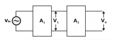 Figure 1
Therefore, overall gain is the product of voltage gain of individual stages.
∴ 
Here,
AV = overall gain
AV1 = voltage gain of 1st stage
AV2 = voltage gain of 2nd stage
Note: If there are ‘n’ number of stages, the product of voltage gains of those ‘n’ stages will be the overall gain of that multistage amplifier circuit.
Effect of Cascading on Bandwidth
- Identical Stages
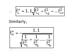
The lower cutoff frequency for the multi stage amplifier is given by:
and the upper cutoff frequency for multi-stage amplifier is given by:
Here,
n = no. of stages
Thus, bandwidth of multi-stage amplifier is
Bw = (fC)high - (fc)low - Non Identical Stages
Here for every gain, separate bandwidth is present.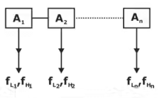 Figure 2: Cascading of non identical stages
Types of Coupling and Comparison
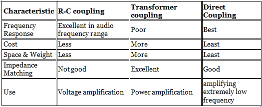
In a multistage amplifier the output of one stage makes the input of the next stage. Normally a network is used between two stages so that a minimum loss of voltage occurs when the signal passes through this network to the next stage. Also, the dc voltage at the output of one stage should not be permitted to go to the input of the next. Otherwise, the biasing of the next stage is disturbed.
The three couplings generally used are
- RC coupling
- Transformer coupling
- direct coupling
Popular Cascading Design
- Cascade Amplifier: (CE – CB configuration)- The cascade amplifier is combination of common-emitter and common-base amplifier. While the C-B amplifier is known for wider bandwidth than the C-E configuration, the low input impedance (10s of Ω) of C-B is a limitation for many applications. The solution is to precede the C-B stage by a low gain C-E stage which has moderately high input impedance (kΩs).
 Figure 3The key to understanding the wide bandwidth of the cascode configuration is the Miller effect.
A common-base configuration is not subject to the Miller effect because the grounded base shields the collector signal from being fed back to the emitter input. Thus, a C-B amplifier has better high frequency response.
The way to reduce the common-emitter gain is to reduce the load resistance. The gain of a C-E amplifier is approximately RC/re. The collector load RC is the resistance of the emitter of the C-B stage loading the C-E state. CE gain amplifier gain is approximately Av = RC/re = 1. This Miller capacitance is Cmiller = Ccbo (1 – Av) = Ccbo (1 – (–1) = 2Ccbo.
We now have a moderately high input impedance C-E stage without suffering the Miller effect, but no C-E stage voltage gain. The C-B stage provides a high voltage gain. The total current gain of cascode is β as current gain of the C-E stage is 1 for the C-B is β.
Note: A cascode amplifier has a high gain, moderately high input impedance, a high output impedance, and a high bandwidth. - Darlington Pair [CC - CC]- It consists of two emitter followers in cascaded mode. The overall gain is close to unity. The main advantage of Darlington amplifier is very large increase in input impedance and an equal decrease in output impedance.
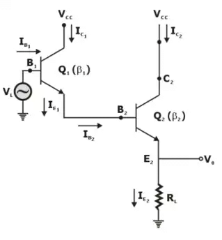 Figure 4
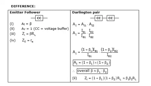
Following are the important characteristics of Darlington pair:
- Extremely high input impedance.
- Extremely high current gain.
- Extremely low output impedance.
Feedback Amplifier
The feedback-amplifier can be defined as an amplifier which has feedback lane that exists between output to input. In this type of amplifier, feedback is the limitation which calculates the sum of feedback given in the following amplifier. The feedback factor is the ratio of the feedback signal and the input signal.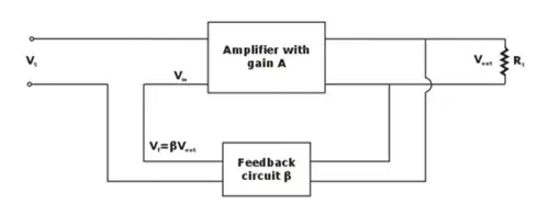 Figure 5: Basic Feedback Amplifier
- Difference between Positive and Negative Feedback:
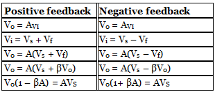 Conclusion
(1) Apf > A > Anf.
Apf. = positive feedback gain
A = without feedback gain.
Anf = negative feedback gain.

Note: Negative feedback theory is applied for stable system like Amplifier.
- Effects of Negative Feedback:
(a) Advantage of Negative Feedback Amplifier
(i) Stability of AC Gain
Suppose there is a small change in the internal resistance ‘re’ of an amplifier then the fractional change of gain with feedback is
Differentiate w.r.t. to A


Note: For a good stable system, sensitivity decreases and desensitivity increases means less sensitive to temperature and noise.
(ii) Increase in Input Impedance
Vi = Vs - Vf
Vi = Vs - βV0
Vi = Vs - βAVi
Vi(1+Aβ) = Vs
Zir = Zi(1 + Aβ)
(iii) Decrease in Output Impedance
V0 + βAV0 = I0Z0
V0(1 + βA) - I0Z0
(iv) Increase in BW
Lower cutoff frequency decreases
f'L = fL/(1+Aβ)
Upper cutoff frequency increases
f'H = (1 + Aβ)fH
BW' = BW(1 + Aβ) - Types of Negative Feedback Amplifier
There are two main types of negative feedback circuits.- Negative Voltage Feedback
- Negative Current Feedback
(a) Negative Voltage Feedback
In this method, the voltage feedback to the input of amplifier is proportional to the output voltage. This is further classified into two types.
(i) Voltage Series Feedback
(ii) Voltage Shunt Feedback
(b) Negative Current Feedback
In this method, the voltage feedback to the input of amplifier is proportional to the output current. This is further classified into two types.
(i) Current Series Feedback
(ii) Current Shunt Feedback
Let’s have a brief description of all.
(a) (i) Voltage Series Feedback
In voltage series feedback circuit, a fraction of the output voltage is applied in series with the input voltage through the feedback circuit.
The following figure shows the block diagram of voltage series feedback.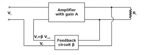 Figure 6: Voltage Series FeedbackAs the feedback circuit is connected in shunt with the output, the output impedance is decreased and due to the series connection with the input, the input impedance is increased.
(ii) Voltage Shunt Feedback
In voltage shunt feedback circuit, a fraction of output voltage is applied in parallel with the input voltage through the feedback network.
The below figure shows block diagram of voltage shunt feedback.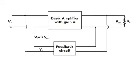 Figure 7: Voltage Shunt Feedback(b) (i) Current Series Feedback
In current series feedback, a fraction of the output voltage is applied in series with the input voltage through the feedback circuit.
The following figure shows the block diagram of current series feedback.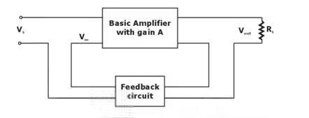 Figure 8: Current Series FeedbackAs the feedback current is connected in series with the output and the input as well, both the output impedance and the input impedance are increased.
(ii) Current Shunt Feedback
In current shunt feedback circuit, a fraction of output voltage is applied in series with the input voltage through the feedback circuit.
The below figure shows the block diagram of current shunt diagram by which it is evident that the feedback circuit is placed in series with the output but in parallel with the input.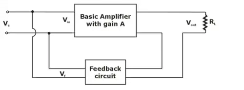 Figure 9: Current Shunt Feedback
Basics of Power Amplifier
- An amplifier is an electronic device used to increase the magnitude of voltage/current/power of an input signal. It takes in a weak electrical signal or waveform and reproduces a similar stronger waveform at the output by using an external power source.
- The power amplifier amplifies the power level of the signal. The amplification is done in the last stage in audio applications. The applications related to radio frequencies employ radio power amplifiers.
- Classification based on Mode of Operation
On the basis of mode of operation i.e. the portion of the input cycle during which collector current flow, the power amplifiers may be classified as
(a) Class A
(b) Class B
(c) Class AB
(d) Class C
(a) CLASS A Power Amplifier
Class A power amplifier is one in which the output current flows for entire cycle of AC input supply. Hence, the complete signal present at the input is amplified at the output. The below figure shows the circuit diagram for class A power amplifier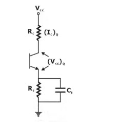 Figure 10: CLASS A Power AmplifierFrom above figure, it can be observed that the transformer is present at the collector as a load. The use of transformer permits the impedance matching, resulting in the transference of maximum power to the load. Example: Loudspeaker.
The operating point of this amplifier is present in the linear region. It is so selected that the current flows for the entire ac input cycle. The below figure explains the selection of operating point.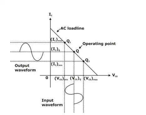 Figure 11: Operating point of CLASS A AmplifierThe output characteristics with operating point Q is shown in figure 11. Here ICQ and VCEQ represents no signal collector current and voltage between collector and emitter respectively. When signal is applied, the Q point steps to Q1 and Q2. The output current increases to (IC)max and decreases to (IC)min. Similarly, the collector emitter voltage increases to (VCE)max and decreases to (VCE)min.
DC power drawn from collector battery VCC is given by:
Pin = voltage × current = VCC(IC)Q
When signal is applied, ac power is developed across load resistors RC which constitutes the ac power output. Here,I = RMS value of ac output current through load.
V = RMS value of ac voltage
Vm = Maximum value of V.
Overall efficiency (η):
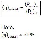
Here, disadvantage of class A power amplifier is that it has low output power and efficiency.
(b) CLASS B Power Amplifier
When the collector current flows only during the positive half cycle of the input signal, the power amplifier is known as class B power Amplifier.
The biasing of the transistor in class B operation is in such a way that at zero signal condition, there will be no collector current. So, when the signal is applied, only the positive half cycle is amplified at the output.
The figure below shows the input and output waveforms during class B operation.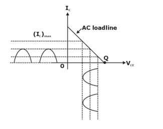 Figure 12: Waveform of CLASS B AmplifierWhen the signal is applied, the circuit is forward biased for the positive half cycle of the input and hence the collector current flows. But during the negative half cycle of the input, the circuit is reverse biased and collector current will be absent. Hence, only positive half cycle is amplified at the output. As the negative half cycle is completely absent, the signal distortion will be high. But when compared to class A power amplifier, the output efficiency is increased.
In order to minimize the disadvantage and achieve low distortion, push pull configuration is used in class B amplifier.Power Efficiency of CLASS B Push Pull Amplifier
The current in each transistor is the average value of half sine loop.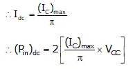
RMS value of collector current
RMS value of output voltage

Now, overall efficiency: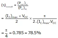
Hence, class B push pull amplifier improves the efficiency than the class A push pull amplifier.
(c) CLASS AB Amplifier
Class B encounters with a important problem of “Cross-over distortion”.
At the zero voltage point, the transistor period of switching over the transistors from one to the other, has its effect which leads to the instances where both the transistors are off at a time. Such instances can be called as flat spot or dead band on the output wave shape.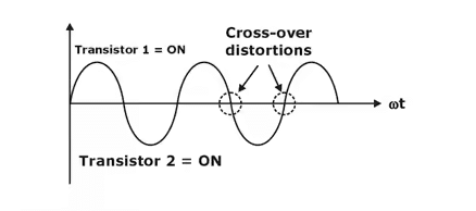 Figure 13The idea leads to the invention of class AB amplifier, which is the combination of both class A and B amplifiers.
As class A has low efficiency problem and class B has distortion problem, therefore class AB resolves both the problems.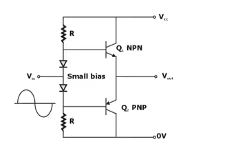 Figure 14: CLASS AB AmplifierThe conduction angle of class AB amplifier is somewhere between 180° to 360° depending upon the operating point selected.
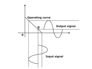 Figure 15: Operating curve of CLASS AB AmplifierEfficiency of class AB is in between 50-60%
(d) CLASS C Amplifier
When the collector current flows for less than half cycle of the input signal, power amplifier is known as class C power amplifier.
Efficiency of class C amplifier is high while linearity is poor.
The conduction angle for class C is less than 180°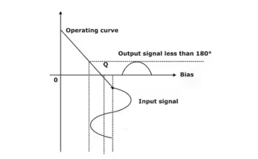 Figure 16: Operating curve of CLASS C Amplifier
|
3 videos|75 docs|64 tests
|
FAQs on Study Notes: Amplifiers - Analog Circuits - Electronics and Communication Engineering (ECE)
| 1. What is the effect of cascading on the bandwidth of a multistage amplifier? |  |
| 2. What are the types of coupling used in multistage amplifiers and how do they compare? |  |
| 3. What is a popular cascading design used in multistage amplifiers? |  |
| 4. What is the power efficiency of a CLASS B push-pull amplifier? |  |
| 5. What are the basics of a power amplifier? |  |


