Lecture 19 - Compensator Design Using Bode Plot - Electrical Engineering (EE) PDF Download

Lecture 19 - Compensator Design Using Bode Plot, Control Systems
1 Compensator Design Using Bode Plot
In this lecture we would revisit the continuous time design techniques using frequency domain since these can be directly applied to design for digital control system by transferring the loop transfer function in z -plane to w-plane.
1.1 Phase lead compensator
If we look at the frequency response of a simple PD controller, it is evident that the magnitude of the compensator continuously grows with the increase in frequency.
The above feature is undesirable because it amplifies high frequency noise that is typically present in any real system.
In lead compensator, a first order pole is added to the denominator of the PD controller at frequencies well higher than the corner frequency of the PD controller.
A typical lead compensator has the following transfer function.
 is the ratio between the pole zero break point (corner) frequencies.
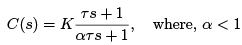
Magnitude of the lead compensator is 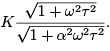 And the phase contributed by the lead compensator is given by
φ = tan−1 ωτ − tan−1 αωτ
Thus a significant amount of phase is still provided with much less amplitude at high frequencies.
The frequency response of a typical lead compensator is shown in Figure 1 where the magnitude varies from 20 log10 K to 20 log10 and maximum phase is always less than 90o (around 60o in general).
Bode Diagram
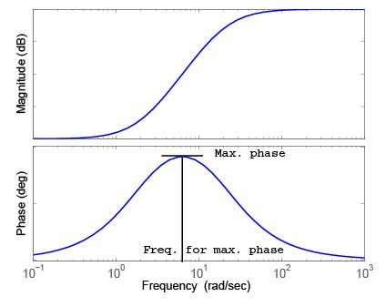
Figure 1: Frequency response of a lead compensator
It can be shown that the frequency where the phase is maximum is given by

The maximum phase corresponds to
The magnitude of C (s) at ωmax is
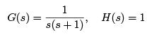
Example 1: Consider the following system
Design a cascade lead compensator so that the phase margin (PM) is at least 45o and steady state error for a unit ramp input is ≤ 0.1.
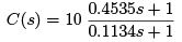
The lead compensator is
When s → 0, C (s) → K .
Steady state error for unit ramp input is
Thus  = 0.1, or K = 10.
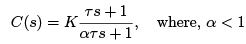
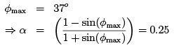
PM of the closed loop system should be 45o. Let the gain crossover frequency of the uncompensated system with K be ωg .
Phase angle at ωg = 3.1 is −90 − tan−1 3.1 = −162o. Thus the PM of the uncompensated system with K is 18o.
If it was possible to add a phase without altering the magnitude, the additional phase lead required to maintain PM=45o is 45o − 18o = 27o at ωg = 3.1 rad/sec.
However, maintaining same low frequency gain and adding a compensator would increase the crossover frequency. As a result of this, the actual phase margin will deviate from the designed one. Thus it is safe to add a safety margin of ∈ to the required phase lead so that if it devaites also, still the phase requirement is met. In general ∈ is chosen between 5o to 15o.
So the additional phase requirement is 27o + 10o = 37o. The lead part of the compensator will provide this additional phase at ωmax.
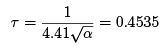
Thus
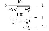
The only parameter left to be designed is τ . To find τ , one should locate the frequency at which the uncompensated system has a logarithmic magnitude of −20 
Select this frequency as the new gain crossover frequency since the compensator provides a gain of 20 at ωmax. Thus

In this case ωmax = ωgnew = 4.41. Thus
The lead compensator is thus
With this compensator actual phase margin of the system becomes 49.6o which meets the design criteria. The corresponding Bode plot is shown in Figure 2
Example 2:
Now let us consider that the system as described in the previous example is sub ject to a sampled data control system with sampling time T = 0.2 sec. Thus
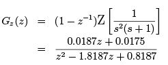
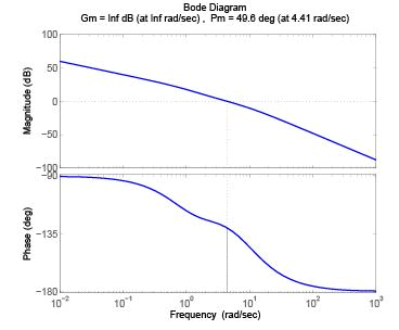
Figure 2: Bode plot of the compensated system for Example 1
The bi-linear transformation
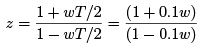
will transfer Gz (z ) into w-plane, as
 [please try the simplification]
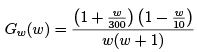
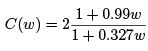
We need first design a phase lead compensator so that PM of the compensated system is at least 500 with Kv = 2 . The compensator in w-plane is
Design steps are as follows.
- K has to be found out from the Kv requirement.
- Compute the gain crossover frequency ωg and phase margin of the uncompensated system after introducing K in the system.
- At ωg check the additional/required phase lead, add safety margin, find out φmax.
Calculate α from the required φmax.
- Since the lead part of the compensator provides a gain of 20 log10
 find out the frequency of the uncompensated system where the logarithmic magnitude is −20 log10 This will be the new gain crossover frequency where the maximum phase lead should occur.
 - Make ωmax = ωgnew
- Calculate τ from the relation
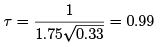
Now,

⇒ K = 2
Using MATLAB command “margin”, phase margin of the system with K = 2 is computed as 31.60 with ωg = 1.26 rad/sec, as shown in Figure 3.
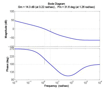
Figure 3: Bode plot of the uncompensated system for Example 2

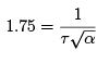
From the frequency response of the system it can be found out that at ω = 1.75 rad/sec, the magnitude of the system is −20 log10 Thus ωgnew = ωmax = 1.75 rad/sec. This gives
Or,
Thus the controller in w-plane is
The Bode plot of the compensated system is shown in Figure 4.
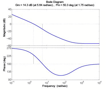
Figure 4: Bode plot of the compensated system for Example 2
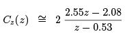
Re-transforming the above controller into z -plane using the relation w =  we get the controller in z -plane, as
FAQs on Lecture 19 - Compensator Design Using Bode Plot - Electrical Engineering (EE)
| 1. What is compensator design and how is it related to Bode Plot? |  |
| 2. How can Bode Plot be used in compensator design? | |
| 3. What are the key considerations in compensator design using Bode Plot? | |
| 4. What are the steps involved in compensator design using Bode Plot? | |
| 5. Can Bode Plot be used for compensator design in any type of system? | |


Top Courses for Electrical Engineering (EE)

Exam
,Previous Year Questions with Solutions
,past year papers
,Important questions
,study material
,mock tests for examination
,shortcuts and tricks
,ppt
,Free
,MCQs
,Viva Questions
,Lecture 19 - Compensator Design Using Bode Plot - Electrical Engineering (EE)
,video lectures
,practice quizzes
,Summary
,Objective type Questions
,Lecture 19 - Compensator Design Using Bode Plot - Electrical Engineering (EE)
,Semester Notes
,Sample Paper
,Extra Questions
,Lecture 19 - Compensator Design Using Bode Plot - Electrical Engineering (EE)
;


Lecture 19 - Compensator Design Using Bode Plot Free PDF Download
Importance of Lecture 19 - Compensator Design Using Bode Plot
Lecture 19 - Compensator Design Using Bode Plot Notes
Lecture 19 - Compensator Design Using Bode Plot Electrical Engineering (EE) Questions
Study Lecture 19 - Compensator Design Using Bode Plot on the App
|
© EduRev
|
Education Revolution
|


|


