Semiconductor ROMs - Electrical Engineering (EE) PDF Download

Objectives
In this lecture you will learn the following
- Introduction to Semiconductor Read Only Memory (ROM)
- NOR based ROM Array
- NAND based ROM Array
31.1 Introduction
Read only memories are used to store constants, control information and program instructions in digital systems. They may also be thought of as components that provide a fixed, specified binary output for every binary input.
The read only memory can also be seen as a simple combinational Boolean network, which produces a specified output value for each input combination, i.e. for each address. Thus storing binary information at a particular address location can be achieved by the presenc e or absence of a data path from the selected row (word line) to the selected column (bit line), which is equivalent to the presence or absence of a device at that particular location.
The two different types of implementations of ROM array are:
- NOR-based ROM array
- NAND-based ROM array
31.2 NOR-based ROM Array
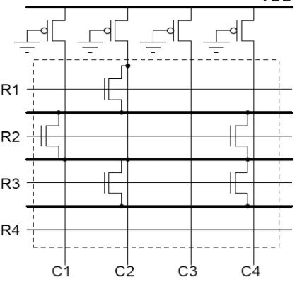
Fig 31.21: NOR-based ROM array
As we know, only one word line is activated at a time by raising tis voltage to VDD, while all other rows are held at a low votlage level. If an active transistor exists at the cross point of a column and the selected row, the column voltage is pulled down to the logic LOW level by that transistor. If no active transistor exists at the cross point, the column voltage is pulled HIGH by the pMOS load device. Thus, a logic "1"-bit is stored as the absence of an active transistor, while a logic "0"-bit is stored as the presence of an active transistor at the cross point. The truth table is shown in Figure 31.22.
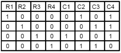
Fig 31.22: Truth Table for Figure 31.21
In an actual ROM layout, the array can be initially manufactured with nMOS transistors at every row-column intersection. The "1"-bit are then realized by omitting the drain or source connection, or the gate electrode of the corresponding nMOS transistors in the final metallization step. Figure 31.23 shows nMOS transistors in a NOR ROM array, forming the intersection of two metal lines and two polysilicon word lines. To save silicon area, the transistors in every two rows are arranged to share a common ground line, also routed in n-type diffusion. To store a "0"-bit at a particular address location, the drain diffusion of the corresponding transistor must be connected to the metal bit line via a metal-to-diffusion contact. Omission of this contact, on the other hand, results in stored "1"-bit.
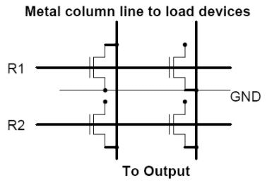
Fig 31.23: Metal column line to load devices
The layout of the ROM array is shown below in Figure 31.24.
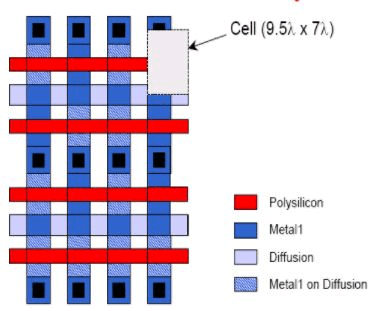
Fig 31.24: Programming using the Active Layer Only
Figure 31.25 shows a different type of NOR ROM layout implementation which is based on deactivation of the nMOS transistor by raising their threshold voltage through channel implants. In this case, all nMOS transistors are alreadly connected to the column lines: therefore, storing a "1"-bit at a particular location by omitting the corresponding the drain contact is not possible. Instead, the nMOS transistor corresponding to the stored "1"-bit can be deactivated, i.e. permanently turned off, by raising its threshold voltage above the VCH level through a selective channel implant during fabrication.
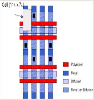
Fig 31.25: Programming using the Contact Layer Only
31.3 NAND-based ROM Array
In this types of ROM array which is shown in Figure 31.31, each bit line consists of a depletion-load NAND gate, driven by some of the row signals, i.e. the word lines. In normal operation, all word lines are held at the logic HIGH voltage level except for the selected line, which is pulled down to logic LOW level. If a transistor exists at the cross point of a column and the selected row, that transistor is turned off and column voltage is pulled HIGH by the load device. On the other hand, if no transistor exists (shorted) at that particular cross point, the column voltage is pulled LOW by the other nMOS transistors in the multi-input NAND structure. Thus, a logic "1"-bit is stored by the presence of a transistor that can be deactivated, while a logic "0"-bit is stored by a shorted or normally ON transistor at the cross point.
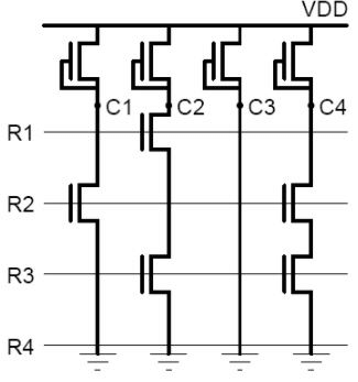
Fig 31.31: NAND-based ROM
As in the NOR ROM case, the NAND-based ROM array can be fabricated initially with a transistor connection present at every row-column intersection. A "0"-bit is then stored by lowering the threshold voltage of the corresponding nMOS transistor at the cross point through a channel implant, so that the transistor remains ON regardless of the gate voltage. The availability of this process step is also the reason why depletion-type nMOS load transistors are used instead of pMOS loads
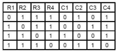
Fig 31.32: Truth table for Fig 31.31
Figures 31.33 and 31.34 show two different types of layout implementations of NAND ROM array. In the implant-mask NAND ROM array, vertical columns of n-type diffusion intersect at regular intervals with horizontal rows of polysilicon, which results in an nMOS transistor at each intersection point. The transistor with threshold voltage implant operate as normally-ON depletion devices, thereby providing a continuous current path regardless of the gate voltage level. Since this structure has no contacts embedded in the array, it is much more compact than the NOR ROM array. However, the access time is usually slower than the NOR ROM, due to multiple series-connected nMOS transistor in each column.
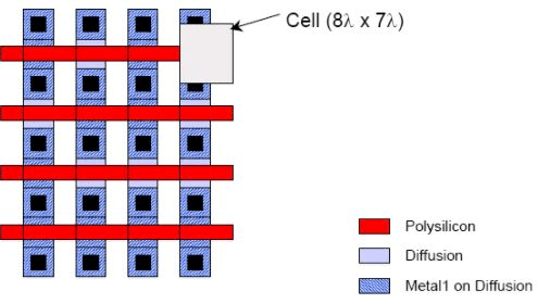
Fig 31.33: Programming using the Metal-1 Layer Only
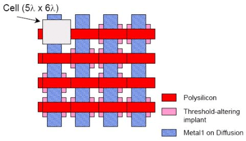
Fig 31.34: Programming using Implants Only
FAQs on Semiconductor ROMs - Electrical Engineering (EE)
| 1. What is a semiconductor ROM? |  |
| 2. How does a semiconductor ROM work? | |
| 3. What are the advantages of using semiconductor ROMs? | |
| 4. Can data be modified or erased from a semiconductor ROM? | |
| 5. What are the different types of semiconductor ROMs? | |


video lectures
,Exam
,Extra Questions
,mock tests for examination
,Previous Year Questions with Solutions
,Important questions
,Semester Notes
,Semiconductor ROMs - Electrical Engineering (EE)
,study material
,ppt
,MCQs
,Summary
,practice quizzes
,Semiconductor ROMs - Electrical Engineering (EE)
,Free
,past year papers
,Semiconductor ROMs - Electrical Engineering (EE)
,Sample Paper
,Viva Questions
,shortcuts and tricks
,Objective type Questions
;


Semiconductor ROMs Free PDF Download
Importance of Semiconductor ROMs
Semiconductor ROMs Notes
Semiconductor ROMs Electrical Engineering (EE) Questions
Study Semiconductor ROMs on the App
|
© EduRev
|
Education Revolution
|


|


