I/O PADs - Electrical Engineering (EE) PDF Download

Objectives
In this lecture you will learn the following
- Introduction
- Electrostatic Discharge
- Output Buffer
- Tri-state Output Circuit
- Latch-Up
- Prevention of Latch-Up
33.1 Introduction
Pad cells surround the rectangular metal patches where external bonds are made. Pads must be sufficiently large and sufficiently spaced apart from each other. There are three types of pad cells, input, output, power (also, tristate, analog). Typical structures inside pad cells should have
- sufficient connection area (eg. 85 x 85 microns) in the pad,
- electrostatic discharge (ESD) protection structures
- interface to internal circuitry
- circuitry specific to input and output pads
Pads are generally arranged around the chip perimeter in a "pad frame". Pad frame will have a signal ring of pads in smaller designs. Lower limit on pad size is minimum size to which a bond wire can be attached; typically 100-150 micrometers. It is also a minimum pitch at which bonding machines can operate.
Input pads of gates of input buffer transistors are susceptible to high voltage build up, so we need to have ESD protection for it. Output pads are expected to drive large capacitance loads, so characteristics of load must be met by proper sizing of output buffer. Due to large transistors, I/O currents are higher and hence Latch-Up may occur. To prevent this, we use guard rings in layout. For area efficiency, I/O transistors should be constructed from several small transistors in parallel. Long gates must be provided to reduce avalanche breakdown tendency
33.2 Electrostatic Discharge (ESD)
ESD damage is usually caused by poor handling procedures. ESD is especially severe in low humidity environments. Electrostatic discharge is a pervasive reliability concern in VLSI circuits. It is a short duration (<200ns) high current (>1A) event that causes irreparable damage. The most common manifestation is the human body ESD event, where a charge of about 0.6uC can be induced on a body capacitance of 100pF, leading to electrostatic potentials of 4KV or greater.
Whenever body comes in contact with plastic or other insulating material, static charge is generated. It can be a very small charge, as low as nano Coulombs, but it can cause potential damage to MOS devices, as voltages are pretty high.
We know that
Q = CV
V = Q/C
V = It/C
Let us consider a modest 1pF capacitor, in which, this 1nC charge is put (can be through a 100uA current for a millisec). This results in
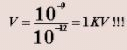
Si O2 breakdown voltage is 109 volts/meter. If gate oxide is about 0.1um thick, say;
Maximum allowable voltage is 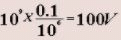
This can easily be generated by walking across a carpet!! A human touch can produce instanteous voltages of 20,000 volts!
A typical solution of the ESD protection problem is to use clamping diodes implemented using MOS transistors with gates tied up to either GND for nMOS transistors, or to VDD for pMOS transistors as shown in Figure 33.21. For normal range of input voltages these transistors are in the OFF state. If the input voltage builds up above (or below) a certain level, one of the transistors starts to conduct clamping the input voltage at the same level.
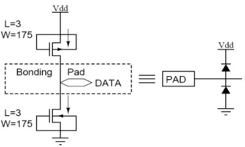
Fig 33.21: Clamping Transistors
These clamping transistors are very big structures consisting of a number of transistors connected in parallel, and are able to sustain significant current. The thick field NMOS used design is not suitable for deep submicron processes, and the thin field oxide NMOS presents oxide breakdown problems while interfacing between blocks with high power supply voltages.
Scaling of VLSI devices have reduced the dimensions of all structures used in ICs and this has increased their susceptibility to ESD damage. Hence ESD protection issues are becoming increasingly important for deep submicron technologies. The gate oxide thicknesses are approaching the tunneling regime of around 35 Angstroms. From an ESD perspective, the important issue is whether the oxide breakdown is reached before the protection devices are able to turn on and protect them!
33.3 Output Buffer
The intra-chip buffer circuits are relatively well known. They are fast, and need only be as big as needed to drive their particular load capacitances. However, in the inter-chip buffer design case, there are some very important limitations. First, these buffers must be able to drive large capacitive loads, as they are driving off-chip signals, which means driving I/O pads, parasitic board capacitances, and capacitances on other chips. Adding a few picofarads of capacitance at the output node is really inconsequential, and shouldnt significantly degrade the propagation delay through this structure. So, the O/P load for worst case design is considered to be 50 times normal load, approximately 50pF. The simplest driver for the output pad consists of a pair of inverters with large transistors in addition to the standard ESD protection circuitry. The driver must be able to supply enough current (must have enough driving capability) to achieve satisfactory rise and fall times (tr, tf) for a given capacitive load. In addition the driver must meet any required DC characteristics regarding the levels of output voltages for a given load type, viz. CMOS or TTL.
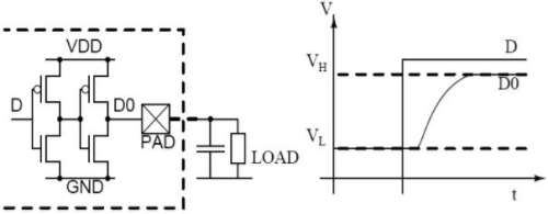
Fig 33.31: Output Buffer
Design method is same as we have already discussed in previous lectures. Optimum number of stages are found for a load capacitance assumed a-priori. Logical effort method can be used to decide sizing.
Second, the voltage across any oxide at any time should not be greater than the supply voltage, which ensures oxide reliability; most process design engineers will not guarantee oxide reliability for oxide voltages greater than the chip VDD. If a low voltage chip is tied to a bus which connects several chips, some with higher supply voltages, then the Input buffer must be designed such that there is no chance of a problem with the oxide.
33.4 Tri-State Output Circuit
The circuits of VLSI chips are designed to be tri-statable as shown in Figure 33.41, which is designed to be driven only when the output enable signal  is asserted. The circuit implementation requires 12 transistors. However in terms of silicon area, this implementation may require a relatively small area since the last stage transistors need not be sized large.
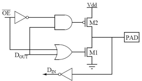
Fig 33.41 Tri-State Output Circuit
33.5 Latch-Up
Large MOS transistors are susceptible to the latch-up effect. In the chip substrate, at the junctions of the p and n material, parasitic pnp and npn bipolar transistors are formed as in the following cross-sectional view shown in Figure 33.51
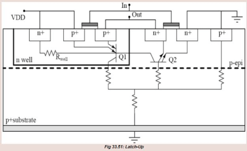
Fig 33.51: Latch-Up
These bipolar transistors form a silicon-controlled rectifier (SRC) with positive feedback as in the following circuit model shown in Figure 33.52
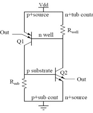
Fig 33.52: SRC With Positive Feedback.
The final result of the latch-up is the formation of a short-circuit (a low impedance path) between VDD and GND which results in the destruction of the MOS transistor.
33.6 Prevention Of Latch-Up
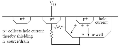
Fig 33.61: Latch-Up Prevention Techniques
The following techniques can be used to prevent latch-up:
- Use p+ guard rings to ground around nMOS transistors and n+ guard rings connected to VDD around pMOS transistors to reduce Rwell and Rsub and to capture injected minority carriers before they reach the base of the parasitic BJTs
- Place substrate and well contacts as close as possible to the source connections
- Use minimum area p-wells (in case of twin-tub technology or n-type substrate) so that the p-well photocurrent can be minimized during transient pulses
- Source diffusion regions of pMOS transistors should be placed so that they lie along equipotential lines when currents flow between VDD and p-wells. In some n-well I/O circuits, wells are eliminated by using only nMOS transistors.
- Avoid the forward biasing of source/drain junctions so as not to inject high currents; the use of a lightly doped epitaxial layer on top of a heavily doped substrate has the effect of shunting lateral currents from the vertical transistor through the low-resistance substrate.
- Layout n- and p-channel transistors such that all nMOS transistors are placed close to GND and pMOS transistors are placed close to VDD rails. Also maintain sufficient spacings between pMOS and nMOS transistors.
FAQs on I/O PADs - Electrical Engineering (EE)
| 1. What are I/O PADs? |  |
| 2. What is the purpose of I/O PADs in electronic devices? | |
| 3. How do I/O PADs ensure proper signal transmission? | |
| 4. Can I/O PADs be customized for specific applications? | |
| 5. What are some challenges in designing I/O PADs? | |


Top Courses for Electrical Engineering (EE)

Objective type Questions
,Sample Paper
,mock tests for examination
,MCQs
,Viva Questions
,Previous Year Questions with Solutions
,video lectures
,ppt
,past year papers
,study material
,Important questions
,Exam
,Summary
,I/O PADs - Electrical Engineering (EE)
,shortcuts and tricks
,practice quizzes
,Extra Questions
,Free
,Semester Notes
,I/O PADs - Electrical Engineering (EE)
,I/O PADs - Electrical Engineering (EE)
;


I/O PADs Free PDF Download
Importance of I/O PADs
I/O PADs Notes
I/O PADs Electrical Engineering (EE) Questions
Study I/O PADs on the App
|
© EduRev
|
Education Revolution
|


|


