Electronic Devices Class 12 Notes Physics
| Table of contents |
|
| Semiconductors |
|
| P-N Junction |
|
| P-N Junction Diode as Rectifier |
|
| Transistor |
|

Semiconductors
Solid semiconductors are substances which have their electrical conductivities lying between that of good conductors and insulators.
Intrinsic semiconductor
Semiconductors without any impurity are called intrinsic semiconductors. For example Germanium (Ge) and silicon (Si). All temperatures near absolute zero, pure Ge and Si behaves like perfect insulators. But their conductivities increases with increase in temperature. For Germanium, the binding energy of an electron in the covalent bond is 0.7 eV. In conductors (metals) free electrons act as charge carriers. In insulators there are no free electrons, while on intrinsic semiconductors both electrons and holes act as charge carriers. When the temperature is increased, the resistance of a conductor increases but the resistance of semiconductor decreases.
Extrinsic Semiconductor
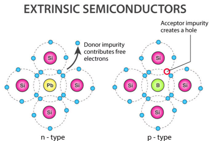
The conductivity of a pure Ge, Si crystal can be considerably increased by adding small quantities of impurities. The addition of controlled amount of impurity to a semiconductor is called doping and a doped Ge or Si crystal is called an extrinsic semiconductor. The quantity of impurity is of the order of one impurity atom in 100 million atoms of Ge or Si.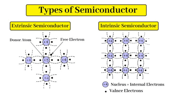 There are two types of extrinsic semiconductors
- n - type semiconductor: Elements like Aresenic (As), Antimony (Sb), Phosphorus (P) are pentavalent i.e. they have five valance electrons while Ge or Si are tetravalent. As the conductivity of Ge or Si doped with pentavalent element is due to free electrons, the semiconductor is called n-type semiconductor. Electrons are major carrier and holes are called minority carriers.
- P - type Semiconductor: If a trivalent impurity like Indium, aluminium, boron is added to Ge or Si then three covalent bonds are formed with 3 Ge atoms. But the fourth valance electron of Ge can not form a covalent bond with indium. The absence of an electron is called a hole. Each hole is regarded as a positive charge at that point.
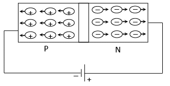
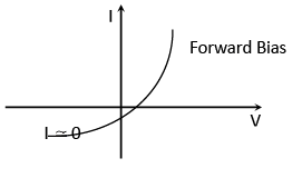
P-N Junction
In this case, when the applied potential difference is greater than the barrier potential difference the diode starts conducting. The direction of hole current is same as that of the conventional current.
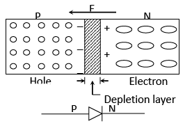
Reverse Biasing
Width of depletion region increased and it acts like an insulator. This current flow due to majority carriers is zero.
P-N Junction Diode as Rectifier
(a) P-N junction Diode as Full wave Rectifier: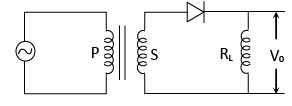
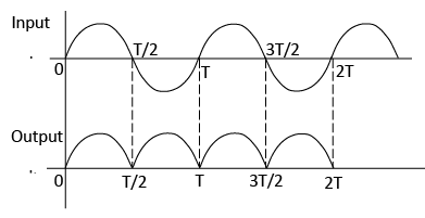
- During the positive half cycle of the input voltage the diode is forward biased hence if conducts and current flows through RL.
- In the negative half cycle of the input voltage the diode is reverse biased and hence no current flows through RL. Thus V0 is unidirectional.
- Hence it is called as half-wave rectifier.
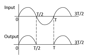
(b) P-N junction Diode as Full wave Rectifier: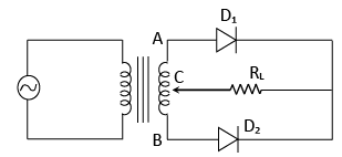
- In the positive half cycle, A is positive w.r.t. C and B has an equal negative voltage.
- In this case D1 is forward biased hence it conducts but D2 is reverse biased and it does not conduct. In the negative half cycle of input voltage; B is positive w.r.t. C and A has an equal negative voltage.
- In this case D2 is forward biased hence it becomes conducting and D1 becomes non-conducting.
- Since the current flows through RL in both halves of the input cycle and since the AC input voltage is falling converted into DC voltage, the arrange is called a full wave rectifier.
Transistor
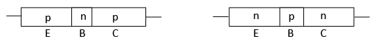
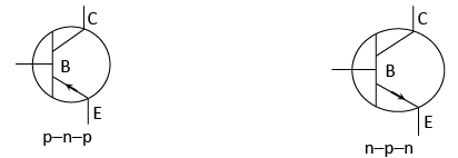
Action in Transistor
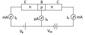
The emitter base junction is forward biased. Some of the electrons combine with the hole in the base and constitute the base current Ib. The electron current flowing from emitter to base forms the emitter current IE. The collector base junction is reverse biased. Hence the electrons are attracted towards the collector, which is maintained at a higher positive potential. The motion of these electrons gives rise to the collector current IC.
According to Kirchoff’s law
IE = IC + IB
Amplifying action of a Transistor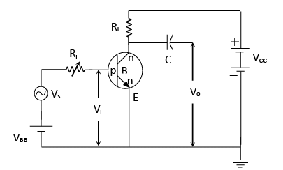 So, power gain = voltage gain × current gain
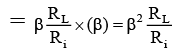
In common Base transistor amplifier,
Logic gates
A digital circuit with one or more input signals but only one output signal is known as logic gate. There are three basic logic gates:
(i) OR gate
(ii) AND Gate
(iii) NOT Gate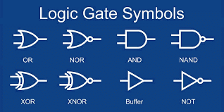
(i) OR gate
The functional statement for ‘OR’ gate is the output (Y) of ‘OR’ gate will be 1 when the input A or B or both are 1. The OR gate in terms of Boolean expression is
A + B= Y
This statement can also be given in the form of a table know as truth table, which is given below 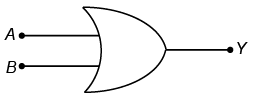 Truth table of two input OR gate:
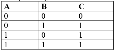
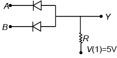
(ii) AND GATE
The functional statement for AND, gate is the output Y of AND gate is 1, if all the inputs simultaneously have the state 1. The AND gate in terms of Boolean expression is Y = A.B
The above function can be stated in the form of the following truth table 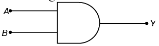
Truth table of AND gate: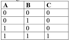
There is no supply current and hence no drop across R only when both A and B are at +5V. Only in that case the output Y goes to supply a voltage of +5V.
 (iii) NOT GATE
The output of the NOT gate is not same as the input, we can say that it performs a negation operation on the input. The truth table is given below 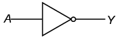 Truth table of NOT gate:
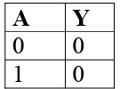
(iv) NOR GATE
If we put an NOT Gate at the output of OR Gate gives a NOT of OR gate or NOR gate. The Boolean equation for NOR gate is Y = A+ B . Truth table for NOR gate can be written as follows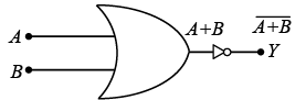 The NOR Truth Table:
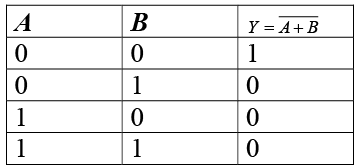 NOR Gate is a universal gate because we can obtain all the possible gates by using this NOR gate as basic building block.
FAQs on Electronic Devices Class 12 Notes Physics
| 1. What is a P-N junction and how does it work? |  |
| 2. What is the function of a P-N junction diode as a rectifier? | |
| 3. What are the different types of rectifiers and how do they differ? | |
| 4. How does a transistor operate and what are its main types? | |
| 5. What are the applications of P-N junction diodes and transistors in electronics? | |


Sample Paper
,study material
,MCQs
,Extra Questions
,Objective type Questions
,Electronic Devices Class 12 Notes Physics
,mock tests for examination
,Free
,Important questions
,Electronic Devices Class 12 Notes Physics
,past year papers
,Electronic Devices Class 12 Notes Physics
,shortcuts and tricks
,Semester Notes
,Previous Year Questions with Solutions
,Summary
,Exam
,Viva Questions
,ppt
,video lectures
,practice quizzes
;


Revision Notes: Electronic Devices Free PDF Download
Importance of Revision Notes: Electronic Devices
Revision Notes: Electronic Devices
Revision Notes: Electronic Devices NEET Questions
Study Revision Notes: Electronic Devices on the App
|
© EduRev
|
Education Revolution
|


|


