JEE Main Previous Year Questions (2016- 2025): Modern Physics- 1 | Physics for Airmen Group X - Airforce X Y / Indian Navy SSR PDF Download
Q.1. A modulating signal is a square wave, as shown in the figure. If the carrier wave is given as c(t) = 2sin(8𝜋t) volts, the modulation index is: (JEE Main 2023)
(1) 1/4
(2) 1/2
(3) 1
(4) 1/3
Ans. (2)
Modulation index μ = Am/Ac
Am = 1 & Ac = 2
μ = 1/2
Q.2. Given below are two statements: one is labelled as Assertion A and the other is labelled as Reason R
Assertion A: Photodiodes are preferably operated in reverse bias condition for light intensity measurement.
Reason R: The current in the forward bias is more than the current in the reverse bias for a 𝑝 − 𝑛 junction diode.
In the light of the above statements, choose the correct answer from the options given below: (JEE Main 2023)
(1) A is true but R is false
(2) A is false but R is true
(3) Both A and R are true and R is the correct explanation of A
(4) Both A and R are true but R is NOT the correct explanation of A
Ans. (4)
Photodiode works in reverse bias and its is used as a intensity detector. (True)
Forward bias current is more as compaired to reverse bias current (True)
Q.3. The logic gate equivalent to the given circuit diagram is : (JEE Main 2023)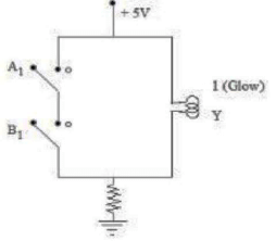 (1) NAND
(2) OR
(3) AND
(4) NOR
Ans. (1)
by truth table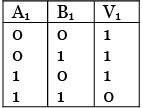
NAND gate
Q.4. Which of the following gives a reversible operation? (2020)
(i) (ii)
(ii) (iii)
(iii) (iv)
(iv) Ans. (4)
Solution.
A logic gate is reversible if it’s input can be recovered from it’s output
Option (1) This is NOR gate, it is not reversible
Option (2) This is OR gate, it is not reversible
Option (3) This is NAND gate, it is not reversible
Option (4) This is NOT gate, it is reversible.
Q.5. In the figure, potential difference between A and B is (2020)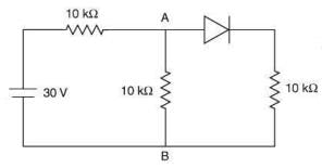 (1) 10 V
(2) 5 V
(3) 15 V
(4) zero
Ans. (1)
Solution.
We have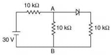 Since, the diode is forward bias so diode behave as short circuit and it will conduct so equivalent circuit will be
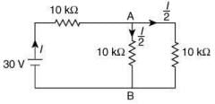 Potential difference between A and B is
Now,
Therefore,
Q.6. Boolean relation at the output stage-Y for the following circuit is (2020) (1)
(1)
(2) A + B
(3) A.B
(4)
Ans. (4)
Solution.
Truth table of input output relation is From truth table, we have
Q.7. In the given circuit, value of Y is (2020)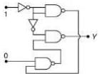 (1) 0
(1) 0
(2) toggles between 0 and 1
(3) will not execute
(4) 1
Ans. (1)
Solution.
Let two input of the given circuit be A and B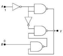 So, output of the circuit is given by
Given that A = 1, B = 0
So, Y = 0+0 = 0
Q.8. Both the diodes used in the circuit shown are assumed to be ideal and have negligible resistance when these are forward biased. Built in potential in each diode is 0.7 V. For the input voltage shown in the figure, the voltage (in Volts) at point A is __________. (2020)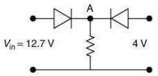 Ans. (12)
Solution.
From given circuit we have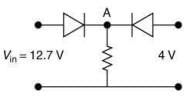 First diode is forward biased and second diode is reversed biased. So, voltage at point A is given by
Q.9. The current I in the network is (2020)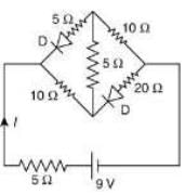 (1) 0.2 A
(2) 0.6 A
(3) 0.3 A
(4) 0
Ans. (3)
Solution.
In the given circuit both diodes are reversed biased. So, they are open circuited.
Redraw the given circuit we have following new figure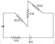 So, current I in the circuit is given by
Here Reff = 5 + 10 + 5 + 10 = 30Ω
Given that V = 9V
Therefore,
Q.10. The circuit shown below is working as an 8 V DC regulated voltage source. When 12 V is used as input, the power dissipated (in mW) in each diode is (considering both zener diodes are identical) ______. (2020)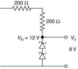 Ans. (40)
Solution.
Given that Vinn = 12V, Vout = 8V
So, voltage across resistance is V = Vin - Vout = 12 - 8 = 4V
Current across resistance is
Total power dissipated across Zener diodes is
P = VI = 8 x 1 x 10-2
= 80 x 10-3 W = 80 mW
Power dissipated across each Zener diode is
P1 = P/2 = 80/2 = 40mW
Q.11. Mobility of electrons in a semiconductor is defined as the ratio of their drift velocity to the applied electric field. If, for an n-type semiconductor, the density of electrons is 1019 m−3 and their mobility is 1.6 m2/(V·s), then the resistivity of the semiconductor (since it is an n-type semiconductor, contribution of holes is ignored) is close to [2019]
(1) 2 Ω·m
(2) 4 Ω·m
(3) 0.4 Ω·m
(4) 0.2 Ω·m
Ans. (3)
Solution.
Current in the semiconductor is,
We know that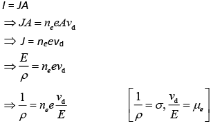

Q.12. Ge and Si diodes start conducting at 0.3 V and 0.7 V, respectively. In the following figure if Ge diode connection is reversed, the value of V0 changes by (assume that the Ge diode has large breakdown voltage) [2019]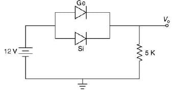
(1) 0.8 V
(2) 0.6 V
(3) 0.2 V
(4) 0.4 V
Ans. (4)
Solution.
In the given circuit,
voltage, V = 12 V
Resistance, R = 5 kΩ
So,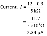
Output voltage
V0 = RI
= (5 × 103) × (2.34 × 10−3)
= 11.7 V
When the connection of Ge diode are reversed then the current will be through Si. Current 

Therefore, output voltage
16 = 1R
= (2.26 × 10−3) × (5 × 103)
= 11.3
The value of V0 = (11.7 – 11.3) V
= 0.4 V
Q.13. To get output 1 at R, for the given logic gate circuit the input values must be [2019]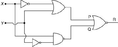
(1) X = 0, Y = 1
(2) X = 1, Y = 1
(3) X = 1, Y = 0
(4) X = 0, Y = 0
Ans. (3)
Solution.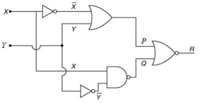
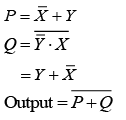
P + Q must be 0
Therefore, Y = 0, X = 1
Q.14. A metal plate of area 1 × 10⁻⁴ m2 is illuminated by a radiation of intensity 16 mW/m2. The work function of the metal is 5 eV. The energy of the incident photons is 10 eV and only 10% of it produces photoelectrons. The number of emitted photo electrons per second and their maximum energy, respectively, will be (1 eV = 1.6 × 10⁻¹⁹ J) [2019]
(1) 1014 and 10 eV
(2) 1012 and 5 eV
(3) 1011 and 5 eV
(4) 1010 and 5 eV
Ans. (4)
Solution.
Energy incident on plate per second = IA
= 1.6 × 10−3 × 1 × 10−4
= 1.6 × 10⁻⁷ W
Kinetic energy
K = hv− ϕ
= 10 – 5 = 5 eV
Now,

⇒ N = 1011
Therefore, number of emitted electrons per second 

Q.15. For the circuit shown below, the current through the Zener diode is [2019]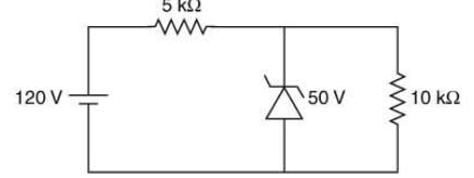
(1) 9 mA
(2) 5 mA
(3) Zero
(4) 14 mA
Ans. (1)
Solution.
If Zener diode does not undergo breakdown
V1 = 120 – 50
= 70
⇒ V = IR
70 = I × 5 × 103 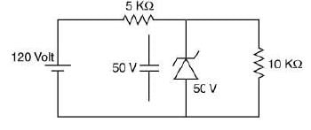

= 14 mA
V1 = 50 V
V1 = I1R
50 = 10 × 103 × I1
Current through diode is
I2 = I – I1
= 14 – 5= 9 mA
Q.16. In the given circuit the current through Zener Diode is close to [2019]
(1) 0.0 mA
(2) 6.0 mA
(3) 6.7 mA
(4) 4.0 mA
Ans. (1)
Solution.
When potential drop across 1500 Ω is 10 V then current flowing through it is [V = IR]
= 6.61 mA
Now, 2 V will be the potential difference across 500 Ω.
Thus, electric current flowing through it is
= 4 mA
So, I2 > I1 this condition is not possible.
Therefore, voltage across Zener diode must be less than 10 V therefore it will not work in break down region and its resistance will be infinite and current through it is equal to 0.
Q.17. The circuit shown below contains two ideal diodes, each with a forward resistance of 50 Ω. If the battery voltage is 6 V, the current through the 100 Ω resistance (in amperes) is [2019]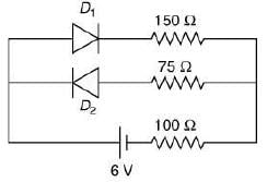
(1) 0.036
(2) 0.020
(3) 0.027
(4) 0.030
Ans. (2)
Solution. 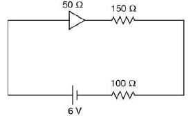
The second diode is reverse biased. Thus, current only flow through first diode and its value is 
Q.18. The output of the given logic circuit is [2019]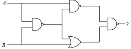


Ans. (3)
Solution.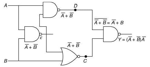
We have,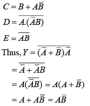
Q.19. In the figure, given that VBB supply can vary from 0 to 5.0 V, VCC = 5 V, βdc = 200, RB = 100 kΩ, RC = l kΩ and VBE = 1.0 V. The minimum base current and the input voltage at which the transistor will go to saturation, will be, respectively [2019]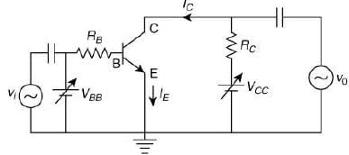
(1) 25 μA and 3.5 V.
(2) 20 μA and 3.5 V.
(3) 25 μA and 2.8 V.
(4) 20 μA and 2.8 V.
Ans. (1)
Solution.
For output, at saturation, VCE = 0
In CE circuit we have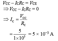
Now,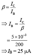
At input side in BE circuit
VBB = IBRB + VBE
= 25 × 10−6 × 100 × 103 + 1
⇒ VBB = 3.5 V
Q.20. In a communication system operating at wavelength 800 nm, only one percent of source frequency is available as signal bandwidth. The number of channels accommodated for transmitting TV signals of band width 6 MHz are (Take velocity of light c = 3 × 10⁸ m/s, h = 6.6 × 10⁻³⁴ J s) [2019]
(1) 3.75 × 10⁶
(2) 3.86 × 10⁶
(3) 6.25 × 10⁵
(4) 4.87 × 10⁵
Ans. (3)
Solution.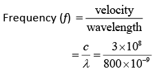
= 3.75 × 10¹⁴ Hz
Usable frequency = 1% of f
Therefore, required number of channel 
= 6.25 × 10⁵
Q.21. A TV transmission tower has a height of 140 m and the height of the receiving antenna is 40 m. What is the maximum distance upto which signals can be broadcasted from this tower in LOS (line-of-sight) mode? (Given: Radius of Earth = 6.4 × 10⁶ m). [2019]
(1) 65 km
(2) 48 km
(3) 80 km
(4) 40 km
Ans. (1)
Solution.
Let hr and hR be the height of transmitter tower and height of receiver respectively.
Maximum distance up to which signal can be broadcasted is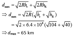
Q.22. The modulation frequency of an AM radio station is 250 Hz, which is 10% of the carrier wave. If another AM station approaches you for license what broadcast frequency will you allot? [2019]
(1) 2750 kHz
(2) 2900 kHz
(3) 2250 kHz
(4) 2000 kHz
Ans. (4)
Solution.
Side band frequency -
AM wave contains three frequency 
- wherein,
fc is carrier frequency,
 are side band frequency.

Range of signal 2250KHz to 2750KHz from option for 2000KHz , from = 200 Hz
range = 1800KHz to 2200KHz.
So, only option (4) lies in the given range.
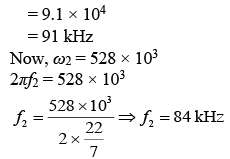
Q.23. An amplitude modulated signal is given by V(t) = 10[1 + 0.3 cos (2.2 × 10⁴t)] sin (5.5 × 10⁵t). Here 't' is in seconds.
The sideband frequencies (in kHz) are (Given: π = 22/7) [2019]
(1) 1785 and 1715.
(2) 892.5 and 857.5.
(3) 178.5 and 171.5.
(4) 89.25 and 85.75.
Ans. (4)
Solution.
We have,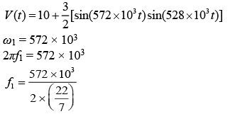
Q.24. An amplitude modulated signal is plotted below: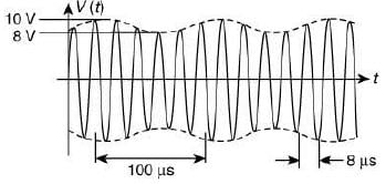
Which one of the following best describes the above signal? [2019]
(1) (9 + sin (2.5π × 105 t)) sin(2π × 104t) V
(2) (1 + 9sin (2π × 104 t)) sin(2.5π × 105t) V
(3) (9 + sin(2π × 104 t))sin(2.5π × 105t) V
(4) (9 + sin(4π × 104 t))sin(5π × 105t) V
Ans. (3)
Solution.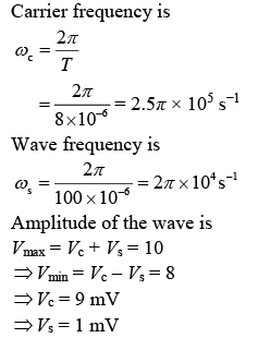

Q.25. A 100V carrier wave is made to vary between 160V and 40V by a modulating signal. What is the modulation index? [2019]
(1) 0.3
(2) 0.5
(3) 0.6
(4) 0.4
Ans. (3)
Solution.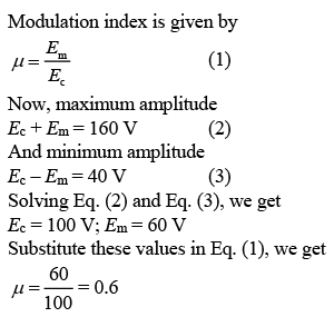
Q.26. To double the covering range of a TV transmission tower, its height should be multiplied by [2019]
(2) 2
(3) 4
Ans. (3)
Solution.
Let d be the cover range of TV tower
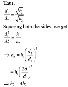
Q.27. The reading of the ammeter for a silicon diode in the given circuit is: [2018]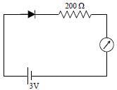
(1) 0
(2) 11.5 mA
(3) 15 mA
(4) 13.5 mA
Ans: (2)
Solution: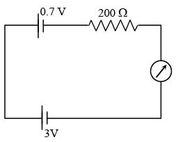

Q.28. A telephonic communication service is working at carrier frequency of 10 GHz. Only 10% of it is utilized for transmission. How many telephonic channels can be transmitted simultaneously if each channel requires a bandwidth of 5 kHz ? [2018]
(1) 2 x 10³
(2) 2 x 10⁴
(3) 2 x 10⁵
(4) 2 x 10⁶
Ans: C
Solution:
No. of telephonic channels that can be transmitted simultaneously
Q.29. In a common emitter configuration with suitable bias, it is given that RL is the load resistance and RBE is small signal dynamic resistance (input side). Then, voltage gain, current gain and power gain are given respectively by:
(β is current gain, IB, IC and IE are respectively base, collector and emitter currents). [2018]
(1)
(2)
(3)
(4)
Ans: (3)
Solution:
Voltage gain
Current gain
Power gain = voltage gain x current gain
Q.30. The number of amplitude modulated broadcast stations that can be accomodated in a 300 kHz band width for the highest modulating frequency 15 kHz will be: [2018]
(1) 10
(2) 15
(3) 20
(4) 8
Ans: A
Solution:
The station will require a band width of 30 kHz
So,
No. of stations = 300/30
= 10
|
201 videos|410 docs|280 tests
|


